IPD060N03L G INFINEON 英飞凌芯片 中文版规格书手册.pdf
需积分: 5 76 浏览量
2023-06-20
11:17:36
上传
评论
收藏 524KB PDF 举报

Type
IPD060N03L G IPF060N03L G
IPS060N03L G IPU060N03L G
OptiMOS
™
3 Power-Transistor
Features
• Fast switching MOSFET for SMPS
• Optimized technology for DC/DC converters
• Qualified according to JEDEC
1)
for target applications
• N-channel, logic level
• Excellent gate charge x R
DS(on)
product (FOM)
• Very low on-resistance R
DS(on)
• Avalanche rated
• Pb-free plating
• Halogen-free according to IEC61249-2-21 *
• Avalanche rated
• Pb-free plating; RoHS compliant
Maximum ratings, at T
j
=25 °C, unless otherwise specified
Parameter Symbol Conditions Unit
Continuous drain current
I
D
V
GS
=10 V, T
C
=25 °C
50 A
V
GS
=10 V, T
C
=100 °C
50
V
GS
=4.5 V, T
C
=25 °C
50
V
GS
=4.5 V,
T
C
=100 °C
43
Pulsed drain current
2)
I
D,pulse
T
C
=25 °C
350
Avalanche current, single pulse
3)
I
AS
T
C
=25 °C
50
Avalanche energy, single pulse
E
AS
I
D
=20 A, R
GS
=25 Ω
60 mJ
Reverse diode dv /dt dv /dt
I
D
=50 A, V
DS
=24 V,
di /dt =200 A/µs,
T
j,max
=175 °C
6 kV/µs
Gate source voltage
V
GS
±20 V
* IPD060N03L G HF available with SP000680632 only in Malacca, Malaysia
IPS060N03L G available in HF
Value
1)
J-STD20 and JESD22
V
DS
30 V
R
DS(on),max
6
mΩ
I
D
50 A
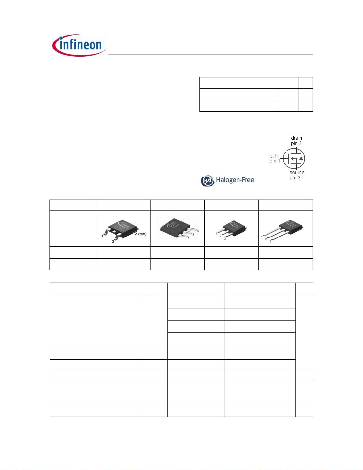
Product Summary
Type
IPD060N03L G IPF060N03L G IPS060N03L G IPU060N03L G
Package
PG-TO252-3 PG-TO252-3-23 PG-TO251-3-11 PG-TO251-3
Marking
060N03L 060N03L 060N03L 060N03L
Rev. 2.1 page 1 2010-04-07
剩余11页未读,继续阅读
资源评论


芯脉芯城
- 粉丝: 3
- 资源: 4031


最新资源
- 使用C语言与python分别实现文件的读写功能
- zephyr sdk package 2
- zephyr sdk package 1
- optimization.ipynb
- 数据库标识码BSM重排序工具、重构标识码工具
- 基于C语言的校园导航系统报告.doc
- __init__.py
- tensorflow-gpu-2.6.5-cp39-cp39-manylinux2010-x86-64.whl
- tensorflow-rocm-2.13.1.600-cp38-cp38-manylinux2014-x86-64.whl
- tensorflow-rocm-2.13.0.570-cp311-cp311-manylinux2014-x86-64.whl
资源上传下载、课程学习等过程中有任何疑问或建议,欢迎提出宝贵意见哦~我们会及时处理!
点击此处反馈


