
07/02/09
www.irf.com 1
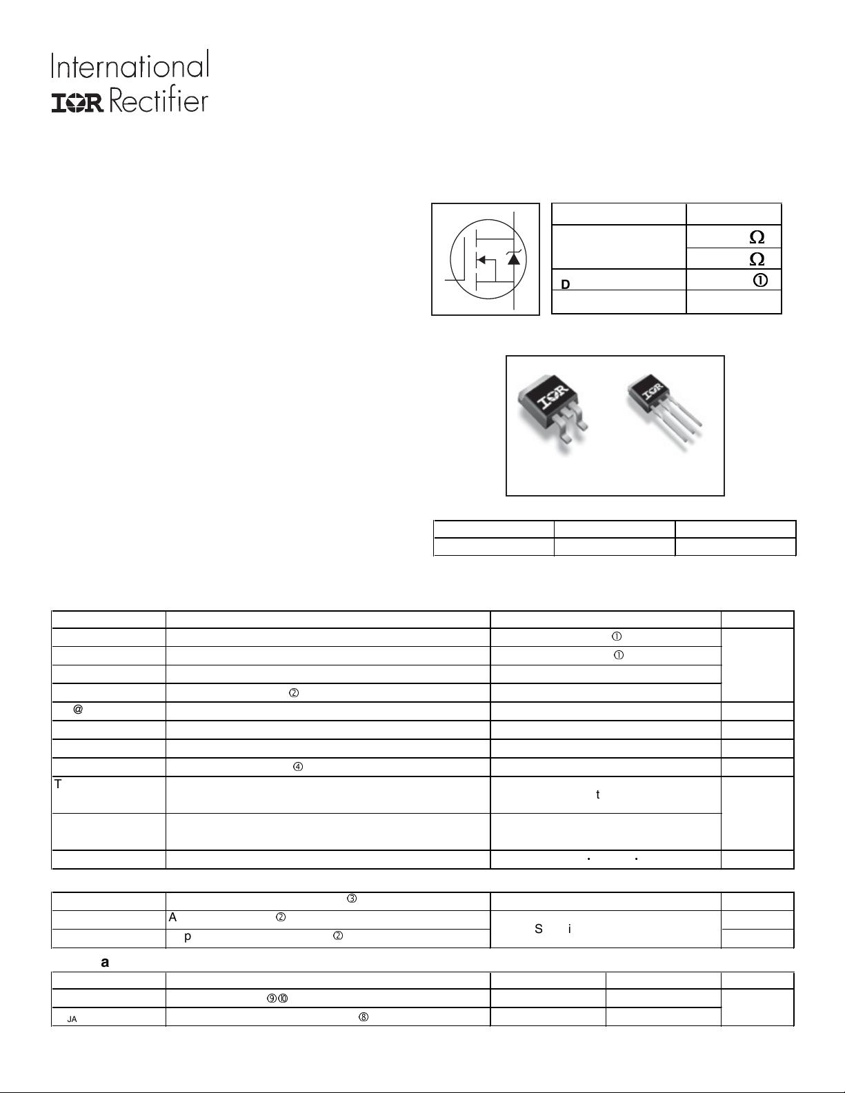
HEXFET
®
Power MOSFET
S
D
G
PD -97364A
IRLS3034PbF
IRLSL3034PbF
GDS
Gate Drain Source
V
DSS
40V
R
DS
(
on
)
typ.
1.4m
:
max.
1.7m
:
I
D
(
Silicon Limited
)
343A
c
I
D
(
Packa
g
e Limited
)
195A
Applications
l DC Motor Drive
l High Efficiency Synchronous Rectification in SMPS
l Uninterruptible Power Supply
l High Speed Power Switching
l Hard Switched and High Frequency Circuits
Benefits
l Optimized for Logic Level Drive
l Very Low R
DS(ON)
at 4.5V V
GS
l Superior R*Q at 4.5V V
GS
l Improved Gate, Avalanche and Dynamic dV/dt
Ruggedness
l Fully Characterized Capacitance and Avalanche
SOA
l Enhanced body diode dV/dt and dI/dt Capability
l Lead-Free
S
D
G
D
D
S
G
D
2
Pak
IRLS3034PbF
TO-262
IRLSL3034PbF
Absolute Maximum Ratings
Symbol Parameter Units
I
D
@ T
C
= 25°C
Continuous Drain Current, V
GS
@ 10V (Silicon Limited)
I
D
@ T
C
= 100°C Continuous Drain Current, V
GS
@ 10V (Silicon Limited)
I
D
@ T
C
= 25°C Continuous Drain Current, V
GS
@ 10V (Package Limited)
I
DM
Pulsed Drain Current
d
P
D
@T
C
= 25°C
Maximum Power Dissipation
W
Linear Derating Factor
W/°C
V
GS
Gate-to-Source Voltage
V
dv/dt
Peak Diode Recovery
f
V/ns
T
J
Operating Junction and
T
STG
Storage Temperature Range
Soldering Temperature, for 10 seconds
(1.6mm from case)
Mounting torque, 6-32 or M3 screw
Avalanche Characteristics
E
AS (Thermally limited)
Sin
g
le Pulse Avalanche Ener
g
y
e
mJ
I
AR
Avalanche Current
d
A
E
AR
Repetitive Avalanche Ener
g
y
d
mJ
Thermal Resistance
Symbol Parameter Typ. Max. Units
R
θJC
Junction-to-Case
kl
–––
0.4
R
θJA
Junction-to-Ambient (PCB Mount)
j
––– 40
-55 to + 175
300
Max.
343
c
243
c
1372
195
See Fig. 14, 15, 22a, 22b,
A
°C
°C/W
255
375
4.6
±20
2.5
10lbf
x
in (1.1N
x
m)
剩余9页未读,继续阅读
资源评论


