TI-TL16C554A.pdf


TL16C554A, TL16C554AI
ASYNCHRONOUS-COMMUNICATIONS ELEMENT
SLLS509E − AUGUST 2001 − REVISED JUNE 2010
1
POST OFFICE BOX 655303 • DALLAS, TEXAS 75265
D Integrated Asynchronous-Communications
Element
D Consists of Four Improved TL16C550C
ACEs Plus Steering Logic
D In FIFO Mode, Each ACE Transmitter and
Receiver Is Buffered With 16-Byte FIFO to
Reduce the Number of Interrupts to CPU
D In TL16C450 Mode, Hold and Shift
Registers Eliminate Need for Precise
Synchronization Between the CPU and
Serial Data
D Up to 16-MHz Clock Rate for up to 1-Mbaud
Operation with V
CC
= 3.3 V and 5 V
D Programmable Baud-Rate Generators
Which Allow Division of Any Input
Reference Clock by 1 to (2
16
−1) and
Generate an Internal 16 × Clock
D Adds or Deletes Standard Asynchronous
Communication Bits (Start, Stop, and
Parity) to or From the Serial-Data Stream
D Independently Controlled Transmit,
Receive, Line Status, and Data Set
Interrupts
D 5-V and 3.3-V Operation
D Fully Programmable Serial Interface
Characteristics:
− 5-, 6-, 7-, or 8-Bit Characters
− Even-, Odd-, or No-Parity Bit
− 1-, 1 1/2-, or 2-Stop Bit Generation
− Baud Generation (DC to 1-Mbit Per
Second)
D False Start Bit Detection
D Complete Status Reporting Capabilities
D Line Break Generation and Detection
D Internal Diagnostic Capabilities:
− Loopback Controls for Communications
Link Fault Isolation
− Break, Parity, Overrun, Framing Error
Simulation
D Fully Prioritized Interrupt System Controls
D Modem Control Functions (CTS, RTS, DSR,
DTR
, RI, and DCD)
D 3-State Outputs Provide TTL Drive
Capabilities for Bidirectional Data Bus and
Control Bus
D Programmable Auto-RTS and Auto-CTS
D CTS Controls Transmitter in Auto-CTS
Mode,
D RCV FIFO Contents and Threshold Control
RTS
in Auto-RTS Mode,
description
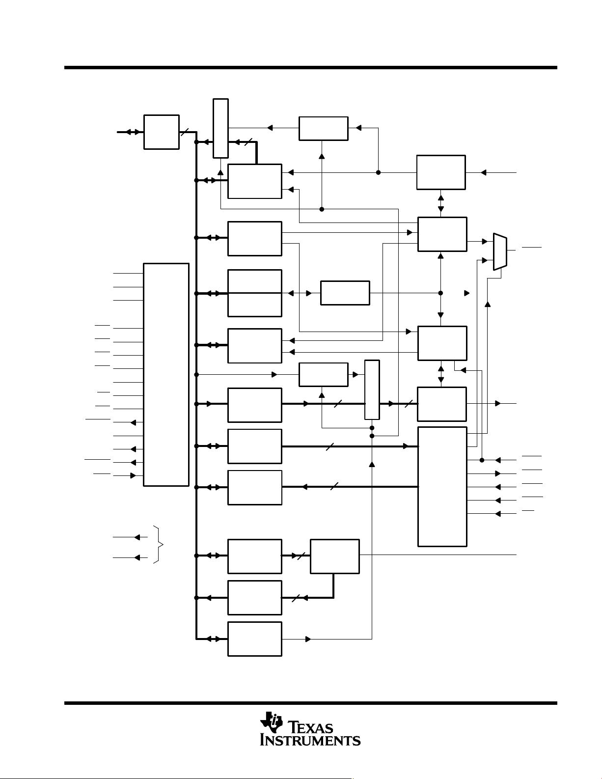
The TL16C554A is an enhanced quadruple version of the TL16C550C asynchronous-communications element
(ACE). Each channel performs serial-to-parallel conversion on data characters received from peripheral
devices or modems and parallel-to-serial conversion on data characters transmitted by the CPU. The complete
status of each channel of the quadruple ACE can be read by the CPU at any time during operation. The
information obtained includes the type and condition of the operation performed and any error conditions
encountered.
The TL16C554A quadruple ACE can be placed in an alternate FIFO mode, which activates the internal FIFOs
to allow 16 bytes (plus three bits of error data per byte in the receiver FIFO) to be stored in both receive and
transmit modes. In the FIFO mode of operation, there is a selectable autoflow control feature that can
significantly reduce software overhead and increase system efficiency by automatically controlling serial-data
flow using RTS
output and CTS input signals. All logic is on the chip to minimize system overhead and maximize
system efficiency. Two terminal functions allow signaling of direct-memory access (DMA) transfers. Each ACE
includes a programmable baud-rate generator that can divide the timing reference clock input by a divisor
between 1 and 2
16
−1.
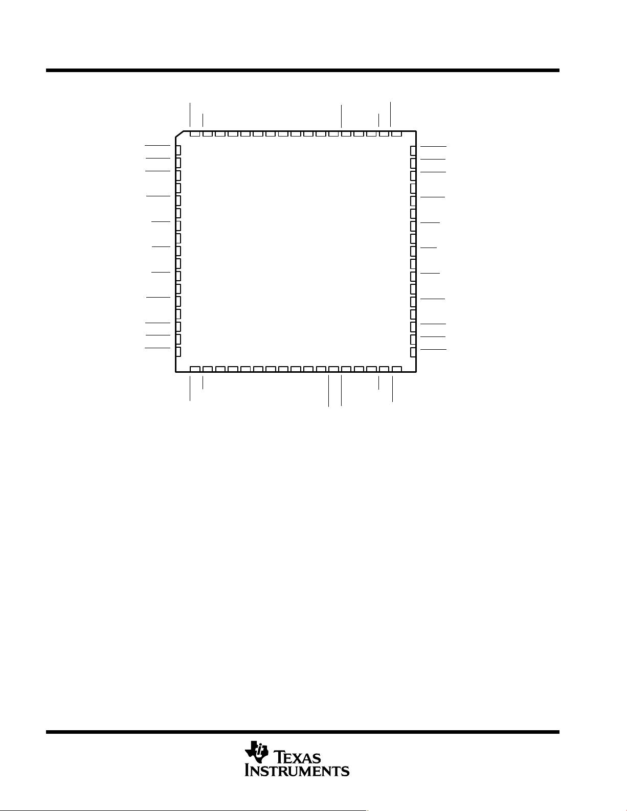
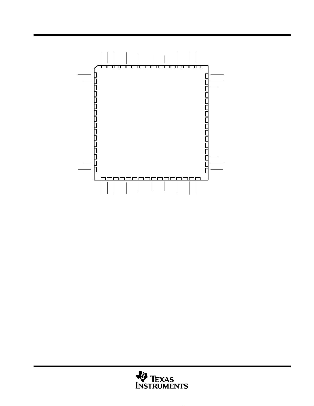
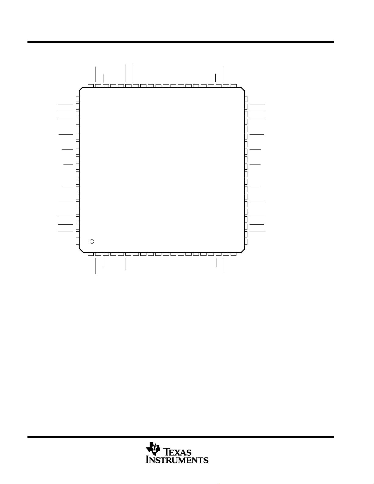
The TL16C554A is available in a 68-pin plastic-leaded chip-carrier (PLCC) FN package, 64-pin plastic quad
flatpack (PQFP) PM package and in an 80-pin (TQFP) PN package.
Please be aware that an important notice concerning availability, standard warranty, and use in critical applications of
Texas Instruments semiconductor products and disclaimers thereto appears at the end of this data sheet.
PRODUCTION DATA information is current as of publication date.
Products conform to specifications per the terms of Texas Instruments
standard warranty. Production processing does not necessarily include
testing of all parameters.
Copyright © 2010, Texas Instruments Incorporated
剩余48页未读,继续阅读
资源评论

 qq_335607272023-02-13#完美解决问题 #运行顺畅 #内容详尽 #全网独家 #注释完整
- m0_745259962023-02-13#完美解决问题 #运行顺畅 #内容详尽 #全网独家 #注释完整
- CSDN_1872023-02-13#完美解决问题 #运行顺畅 #内容详尽 #全网独家 #注释完整
- 2301_763960562023-02-13#完美解决问题 #运行顺畅 #内容详尽 #全网独家 #注释完整


