TI-DS90CR485.pdf

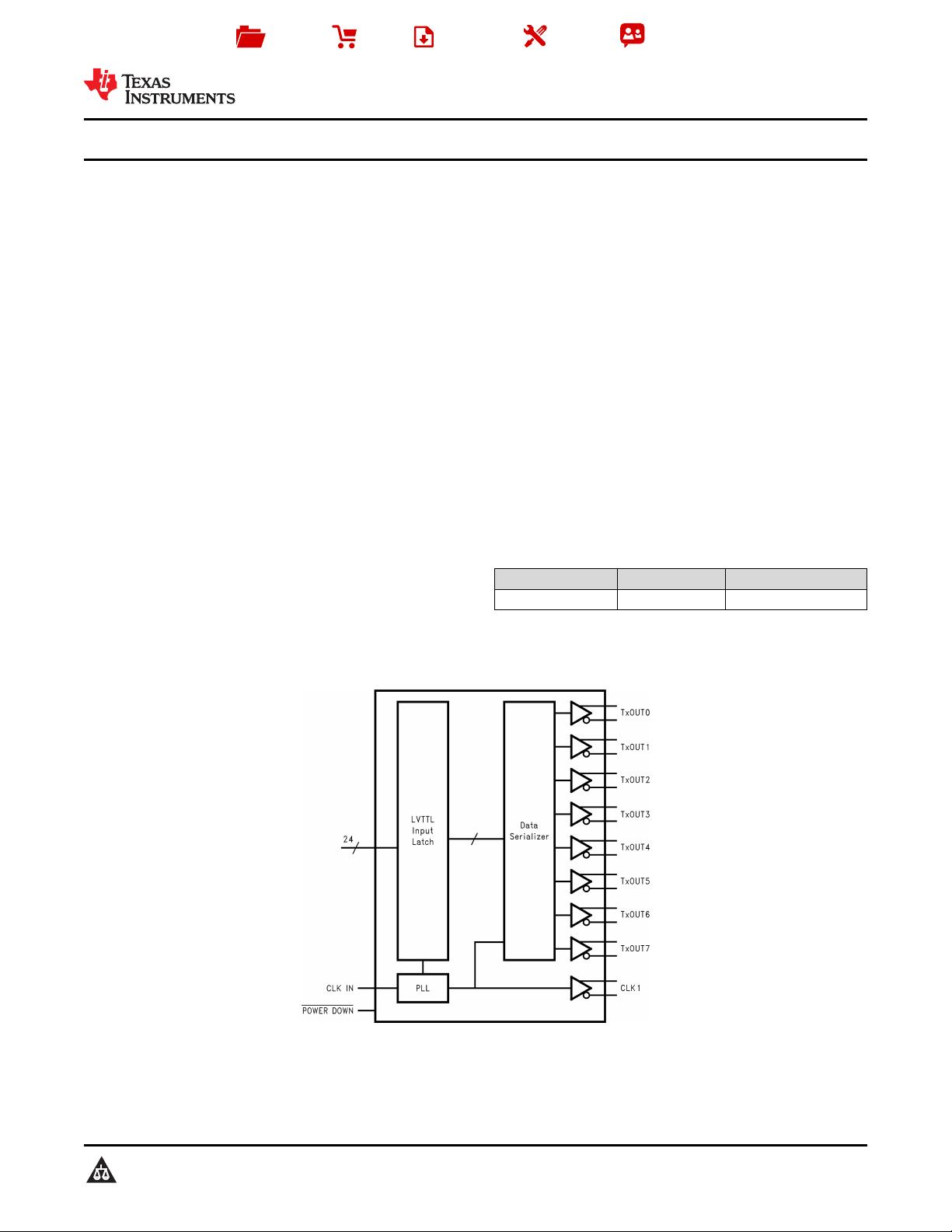
TI公司的DS90CR485是一款高性能的133MHz、48位通道链路串行器,设计用于在高速点对点应用中解决电磁干扰(EMI)和连接器尺寸问题。这款器件能够将24位双沿输入(LVCMOS/LVTTL)的数据在每个时钟周期内锁存为48位,并通过8条低电压差分信号(LVDS)流进行串行化。其工作速率高达6.384 Gbps,显著提高了数据传输效率。
DS90CR485支持66MHz至133MHz的输入时钟频率,具有预加重功能,能减少电缆负载效应,同时通过直流平衡技术减小了互符号干扰(ISI)失真。该器件的输入端口兼容3V的LVCMOS/LVTTL标准,功耗低,仅需2.5V电源。其流线型引脚布局简化了PCB布线,采用100引脚TQFP封装,符合TIA/EIA-644-A LVDS标准,确保了与行业标准的兼容性。
此外,DS90CR485还通过第9个LVDS链路并行传输相位锁定的发送时钟,与数据流同步。这种双沿输入触发方式在时钟的上升沿和下降沿捕获数据,减少了所需的引脚数量,降低了PCB设计复杂度。该器件与DS90CR486通道链路接收器兼容,并向后兼容其他通道链路接收器,如DS90CR482和DS90CR484。
总体而言,DS90CR485串行器是高带宽应用的理想选择,例如背板通信和电缆互连。它通过减少宽TTL总线到少量LVDS线路,有效地减小了电缆和连接器的尺寸和成本,从而降低了系统的整体成本。由于其高数据速率和优化的信号完整性特性,DS90CR485在需要大量数据传输的系统中表现出色,特别是在那些对空间和电磁兼容性有严格要求的应用中。
在设计过程中,应参考TI提供的数据手册、技术支持和社区资源,确保正确使用DS90CR485。请注意,数据表末尾的重要通知包含了关于可用性、保修、安全关键应用使用、知识产权问题和其他重要免责声明的信息。对于生产数据,建议查阅最新的修订版数据表以获取最新信息。
Product
Folder
Order
Now
Technical
Documents
Tools &
Software
Support &
Community
An IMPORTANT NOTICE at the end of this data sheet addresses availability, warranty, changes, use in safety-critical applications,
intellectual property matters and other important disclaimers. PRODUCTION DATA.
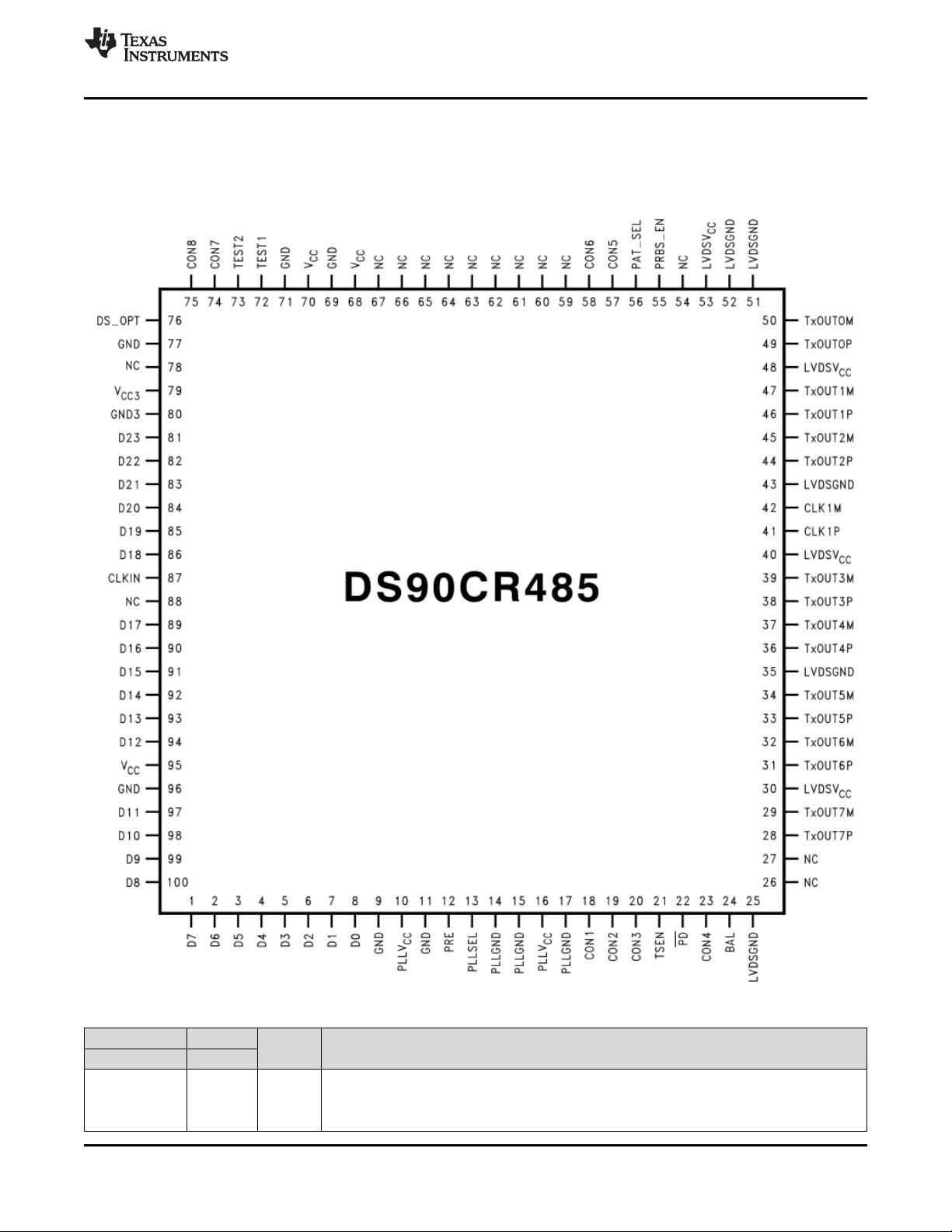
DS90CR485
SNLS143E –FEBRUARY 2003–REVISED SEPTEMBER 2019
DS90CR485 133-MHz, 48-Bit Channel Link Serializer (6.384 Gbps)
1
1 Features
1
• Up to 6.384-Gbps Throughput
• 66-MHz to 133-MHz Input Clock Support
• Reduces Cable and Connector Size and Cost
• Pre-Emphasis Reduces Cable Loading Effects
• DC Balance Reduces ISI Distortion
• 24-Bit Double Edge Inputs
• 3-V Tolerant LVCMOS/LVTTL Inputs
• Low Power, 2.5-V Supply
• Flow-Through Pinout
• 100-Pin TQFP Package
• Conforms With TIA/EIA-644-A LVDS Standard
2 Applications
• Backplane
• Cable Interconnect
3 Description
The DS90CR485 device serializes the 24
LVCMOS/LVTTL double-edge inputs (48 bits data
latched in per clock cycle) onto eight Low Voltage
Differential Signaling (LVDS) streams. A phase-
locked transmit clock is also in parallel with the data
streams over a 9th LVDS link. The reduction of the
wide TTL bus to a few LVDS lines reduces cable and
connector size and cost. The double-edge input
strobes data on both the rising and falling edges of
the clock. This minimizes the pin count required and
simplifies PCB routing between the host chip and the
serializer.
This chip can help resolve EMI and interconnect size
problems for high throughput point-to-point
applications.
The DS90CR485 is compatible with the DS90CR486
Channel-Link receiver. The device is also backward-
compatible with other Channel-Link receivers such as
the DS90CR482 and DS90CR484.
Device Information
(1)
PART NUMBER PACKAGE BODY SIZE (NOM)
DS90CR485 TQFP (100) 14.00 mm × 14.00 mm
(1) For all available packages, see the orderable addendum at
the end of the data sheet.
Generalized Block Diagram
剩余26页未读,继续阅读
113 浏览量
2023-02-08 上传
2023-02-08 上传
152 浏览量
184 浏览量
200 浏览量
2022-12-16 上传
156 浏览量
142 浏览量
175 浏览量
164 浏览量
2024-03-14 上传
130 浏览量
2022-03-08 上传
124 浏览量
127 浏览量
138 浏览量
152 浏览量
164 浏览量
182 浏览量
资源评论

 2301_763960562023-02-15#完美解决问题 #运行顺畅 #内容详尽 #全网独家 #注释完整

不觉明了
- 粉丝: 7423
- 资源: 5764


最新资源
- 微信社团小程序ssm-微信小程序毕业项目,适合计算机毕-设、实训项目、大作业学习.rar
- 校园综合服务小程序+ssm-微信小程序毕业项目,适合计算机毕-设、实训项目、大作业学习.rar
- 微信平台签到系统的设计与实现springboot-微信小程序毕业项目,适合计算机毕-设、实训项目、大作业学习.rar
- 微信小程序的高校党费收缴系统ssm-微信小程序毕业项目,适合计算机毕-设、实训项目、大作业学习.rar
- 学生活动管理系统+ssm-微信小程序毕业项目,适合计算机毕-设、实训项目、大作业学习.rar
- 新闻资讯微信小程序开发后端+php-微信小程序毕业项目,适合计算机毕-设、实训项目、大作业学习.rar
- 自动驾驶控制器,基于分布式驱动电动汽车的四轮侧偏刚度估计,采用容积卡尔曼(ckf)进行估计,能够很好地估计汽车行驶过程中的侧偏刚度,并与转化的侧向轮胎力进行比较,具有很好的估计效果 模型中第一个模块
- 新闻资讯系统设计+springboot-微信小程序毕业项目,适合计算机毕-设、实训项目、大作业学习.rar
- 数据结构PTA理论题答案.zip
- 微信小程序的驾校预约管理系统--论文-微信小程序毕业项目,适合计算机毕-设、实训项目、大作业学习.zip
- 微信小程序的英语学习激励系统--论文-微信小程序毕业项目,适合计算机毕-设、实训项目、大作业学习.zip
- 微信小程序基于BS模式的学生实习与就业管理系统设计与实现springboot-微信小程序毕业项目,适合计算机毕-设、实训项目、大作业学习.rar
- 学生知识成果展示与交流+ssm-微信小程序毕业项目,适合计算机毕-设、实训项目、大作业学习.rar
- 学习自律养成小程序+ssm-微信小程序毕业项目,适合计算机毕-设、实训项目、大作业学习.rar
- 医院挂号系统设计与实现+ssm-微信小程序毕业项目,适合计算机毕-设、实训项目、大作业学习.rar
- 微信小程序评分小程序ssm-微信小程序毕业项目,适合计算机毕-设、实训项目、大作业学习.rar
