没有合适的资源?快使用搜索试试~ 我知道了~
National-Semiconductor-NM27C256.pdf
需积分: 10 0 下载量 188 浏览量
2022-12-11
13:45:17
上传
评论 4
收藏 174KB PDF 举报
温馨提示
试读
12页
National-Semiconductor-NM27C256.pdf
资源推荐
资源详情
资源评论
TL/D/10833
NM27C256 262,144-Bit (32K x 8) High Performance CMOS EPROM
December 1993
NM27C256
262,144-Bit (32K x 8) High Performance CMOS EPROM
General Description
The NM27C256 is a 256K Electrically Programmable Read
Only Memory. It is manufactured in National’s latest CMOS
split gate EPROM technology which enables it to operate at
speeds as fast as 120 ns access time over the full operating
range.
The NM27C256 provides microprocessor-based systems
extensive storage capacity for large portions of operating
system and application software. Its 120 ns access time
provides high speed operation with high-performance CPUs.
The NM27C256 offers a single chip solution for the code
storage requirements of 100% firmware-based equipment.
Frequently-used software routines are quickly executed
from EPROM storage, greatly enhancing system utility.
The NM27C256, is configured in the standard EPROM pin-
out which provides an easy upgrade path for systems which
are currently using standard EPROMs.
The NM27C256 is one member of a high density EPROM
Family which range in densities up to 4 Mb.
Features
Y
High performance CMOS
Ð 120 ns access time
Y
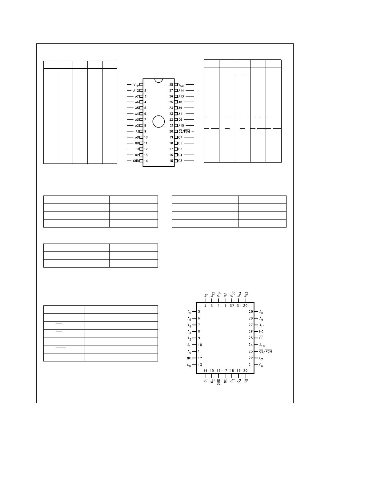
JEDEC standard pin configuration
Ð 28-pin DIP package
Ð 32-pin chip carrier
Y
Drop-in replacement for 27C256 or 27256
Y
Manufacturer’s identification code
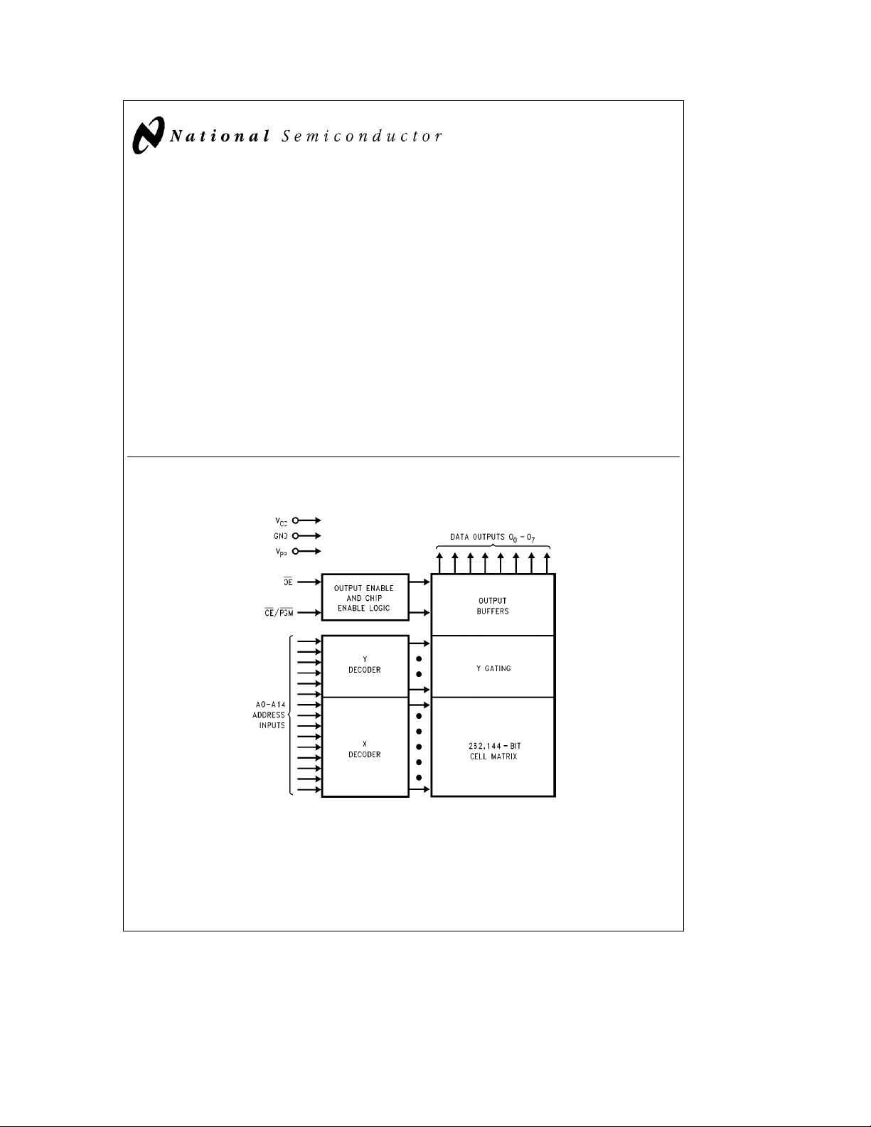
Block Diagram
TL/D/10833–1
TRI-STATE
É
is a registered trademark of National Semiconductor Corporation.
HPC
TM
is a trademark of National Semiconductor Corporation.
C
1995 National Semiconductor Corporation RRD-B30M65/Printed in U. S. A.
Connection Diagrams
27C080 27C040 27C020 27C010 27C512
A19 XX/V
PP
XX/V
PP
XX/V
PP
A16 A16 A16 A16
A15 A15 A15 A15 A15
A12 A12 A12 A12 A12
A7 A7 A7 A7 A7
A6 A6 A6 A6 A6
A5 A5 A5 A5 A5
A4 A4 A4 A4 A4
A3 A3 A3 A3 A3
A2 A2 A2 A2 A2
A1 A1 A1 A1 A1
A0 A0 A0 A0 A0
O0 O0 O0 O0 O0
O1 O1 O1 O1 O1
O2 O2 O2 O2 O2
GND GND GND GND GND
DIP
NM27C256
TL/D/10833–2
27C512 27C010 27C020 27C040 27C080
V
CC
V
CC
V
CC
V
CC
XX/PGM XX/PGM A18 A18
V
CC
XX A17 A17 A17
A14 A14 A14 A14 A14
A13 A13 A13 A13 A13
A8 A8 A8 A8 A8
A9 A9 A9 A9 A9
A11 A11 A11 A11 A11
OE
/V
PP
OE OE OE OE/V
PP
A10 A10 A10 A10 A10
CE
/PGM CE CE CE/PGM CE/PGM
O7 O7 O7 O7 O7
O6 O6 O6 O6 O6
O5 O5 O5 O5 O5
O4 O4 O4 O4 O4
O3 O3 O3 O3 O3
Note: Compatible EPROM pin configurations are shown in the blocks adjacent to the NM27C256 pins.
Commercial Temp. Range (0
§
Cto
a
70
§
C)
V
CC
e
5V
g
10%
Parameter/Order Number Access Time (ns)
NM27C256 Q, N, V 120 120
NM27C256 Q, N, V 150 150
NM27C256 Q, N, V 200 200
Military Temp. Range (
b
55
§
Cto
a
125
§
C)
V
CC
e
5V
g
10%
Parameter/Order Number Access Time (ns)
NM27C256 QM 150 150
NM27C256 QM 250 250
Extended Temp. Range (
b
40
§
Cto
a
85
§
C)
V
CC
e
5V
g
10%
Parameter/Order Number Access Time (ns)
NM27C256 QE, NE, VE 120 120
NM27C256 QE, NE, VE 150 150
NM27C256 QE, NE, VE 200 200
Note: Surface mount PLCC package available for commercial and extended
temperature ranges only.
Package Types: NM27C256 Q, N, V XXX
Q
e
Quartz-Windowed Ceramic DIP
N
e
Plastic OTP DIP
V
e
Surface-Mount PLCC
#
All packages conform to the JEDEC standard.
#
All versions are guaranteed to function for slower
speeds.
Pin Names
Symbol Description
A0– A14 Addresses
CE Chip Enable
OE Output Enable
O0– O7 Outputs
PGM Program
XX Don’t Care (during Read)
PLCC
TL/D/10833–3
Top
2
Absolute Maximum Ratings (Note 1)
If Military/Aerospace specified devices are required,
please contact the National Semiconductor Sales
Office/Distributors for availability and specifications.
Storage Temperature
b
65
§
Cto
a
150
§
C
All Input Voltages except A9 with
Respect to Ground
b
0.6V to
a
7V
V
PP
and A9 with Respect
to Ground
b
0.7V to
a
14V
V
CC
Supply Voltage with
Respect to Ground
b
0.6V to
a
7V
ESD Protection
l
2000V
All Output Voltages with
Respect to Ground V
CC
a
1.0V to GND
b
0.6V
Operating Range
Range Temperature V
CC
Comm’l 0
§
Cto
a
70
§
C
a
5V
g
10%
Industrial
b
40
§
Cto
a
85
§
C
a
5V
g
10%
Military
b
55
§
Cto
a
125
§
C
a
5V
g
10%
Read Operation
DC Electrical Characteristics
Over Operating Range with V
PP
e
V
CC
Symbol Parameter Test Conditions Min Max Units
V
IL
Input Low Level
b
0.5 0.8 V
V
IH
Input High Level 2.0 V
CC
a
1V
V
OL
Output Low Voltage I
OL
e
2.1 mA 0.4 V
V
OH
Output High Voltage I
OH
eb
2.5 mA 3.5 V
I
SB1
V
CC
Standby Current CE
e
V
CC
g
0.3V
100 mA
(Note 11) (CMOS)
I
SB2
V
CC
Standby Current (TTL) CE
e
V
IH
1mA
I
CC1
V
CC
Active Current CE
e
OE
e
V
IL
,f
e
5 MHz
35 mA
TTL Inputs Inputs
e
V
IH
or V
IL
, I/O
e
0mA
I
PP
V
PP
Supply Current V
PP
e
V
CC
10 mA
V
PP
V
PP
Read Voltage V
CC
b
0.7 V
CC
V
I
LI
Input Load Current V
IN
e
5.5V or GND
b
11mA
I
LO
Output Leakage Current V
OUT
e
5.5V or GND
b
10 10 mA
AC Electrical Characteristics Over Operating Range with V
PP
e
V
CC
Symbol Parameter
100 120 150 200
Units
Min Max Min Max Min Max Min Max
t
ACC
Address to Output Delay 100 120 150 200
ns
t
CE
CE to Output Delay 100 120 150 200
t
OE
OE to Output Delay 50 50 50 50
t
DF
Output Disable to
30 35 45 55
(Note 2) Output Float
t
OH
Output Hold from Addresses,
(Note 2) CE
or OE,0000
Whichever Occurred First
3
剩余11页未读,继续阅读
资源评论
不觉明了
- 粉丝: 3117
- 资源: 5348
上传资源 快速赚钱
- 我的内容管理 展开
- 我的资源 快来上传第一个资源
- 我的收益 登录查看自己的收益
- 我的积分 登录查看自己的积分
- 我的C币 登录后查看C币余额
- 我的收藏
- 我的下载
- 下载帮助
最新资源
- 最全空间计量实证方法(空间杜宾模型和检验以及结果解释文档).txt
- 5uonly.apk
- 蓝桥杯Python组的历年真题
- 2023-04-06-项目笔记 - 第一百十九阶段 - 4.4.2.117全局变量的作用域-117 -2024.04.30
- 前端开发技术实验报告:内含4四实验&实验报告
- Highlight Plus v20.0.1
- 林周瑜-论文.docx
- 基于MIC+NE555光敏电阻的声光控电路Multisim仿真原理图
- 基于JSP毕业设计-基于WEB操作系统课程教学网站的设计与实现(源代码+论文).zip
资源上传下载、课程学习等过程中有任何疑问或建议,欢迎提出宝贵意见哦~我们会及时处理!
点击此处反馈
安全验证
文档复制为VIP权益,开通VIP直接复制
信息提交成功