没有合适的资源?快使用搜索试试~ 我知道了~
National-Semiconductor-LM4843MH.pdf
需积分: 5 0 下载量 194 浏览量
2022-12-03
19:24:56
上传
评论 4
收藏 553KB PDF 举报
温馨提示
试读
19页
National-Semiconductor-LM4843MH.pdf
资源推荐
资源详情
资源评论
LM4843
Stereo 2W Audio Power Amplifiers
with DC Volume Control
General Description
The LM4843 is a monolithic integrated circuit that provides
DC volume control, and stereo bridged audio power amplifi-
ers capable of producing 2W into 4Ω (Note 1) with less than
1.0% THD or 2.2W into 3Ω (Note 2) with less than 1.0%
THD.
Boomer
®
audio integrated circuits were designed specifically
to provide high quality audio while requiring a minimum
amount of external components. The LM4843 incorporates a
DC volume control with stereo bridged audio power amplifi-
ers making it optimally suited for multimedia monitors, por-
table radios, desktop, and portable computer applications.
The LM4843 features an externally controlled, low-power
consumption shutdown mode, and both a power amplifier
and headphone mute for maximum system flexibility and
performance.
Note 1: When properly mounted to the circuit board, the LM4843MH will
deliver 2W into 4Ω. See the Application Information section for LM4843MH
usage information.
Note 2: LM4843MH that has been properly mounted to the circuit board and
forced-air cooled will deliver 2.2W into 3Ω.
Key Specifications
n P
O
at 1% THD+N
n into 3Ω 2.2W (typ)
n into 4Ω 2.0W (typ)
n into 8Ω 1.1W (typ)
n Shutdown current 0.7µA (typ)
Features
n Acoustically Enhanced DC Volume Control Taper
n Stereo bridged power amplifiers
n “Click and pop” suppression circuitry
n Thermal shutdown protection circuitry
Applications
n Portable and Desktop Computers
n Multimedia Monitors
n Portable Radios, PDAs, and Portable TVs
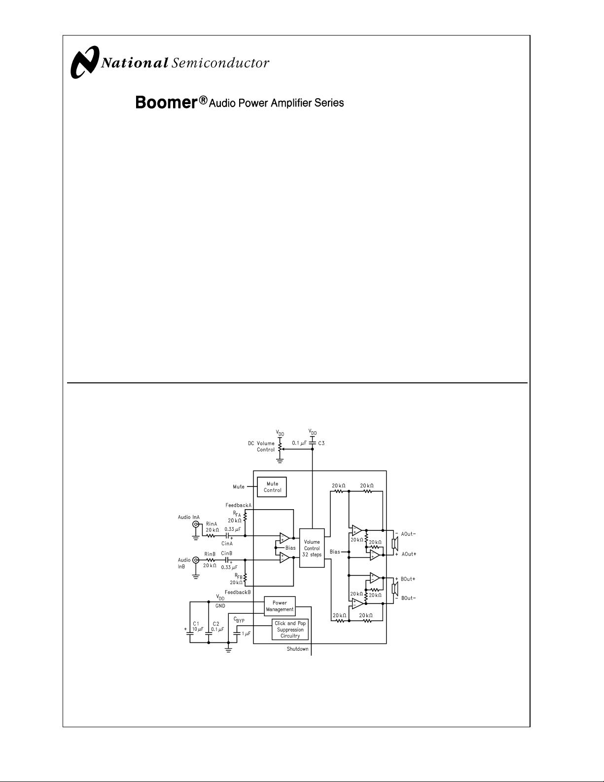
Block Diagram
Boomer
®
is a registered trademark of NationalSemiconductor Corporation.
20038389
FIGURE 1. LM4843 Block Diagram
July 2002
LM4843 Stereo 2W Audio Power Amplifiers with DC Volume Control
© 2002 National Semiconductor Corporation DS200383 www.national.com
Connection Diagram
Standard LM4843MH
20038387
Top View
Order Number LM4843MH
See NS Package Number MXA20
LM4843
www.national.com 2
Absolute Maximum Ratings (Note 10)
If Military/Aerospace specified devices are required,
please contact the National Semiconductor Sales Office/
Distributors for availability and specifications.
Supply Voltage 6.0V
Storage Temperature -65˚C to +150˚C
Input Voltage −0.3V to V
DD
+0.3V
Power Dissipation Internally limited
ESD Susceptibility (Note 12) 2000V
ESD Susceptibility (Note 13) 200V
Junction Temperature 150˚C
Soldering Information
Small Outline Package
Vapor Phase (60 sec.) 215˚C
Infrared (15 sec.) 220˚C
See AN-450 “Surface Mounting and their Effects on
Product Reliability” for other methods of soldering surface
mount devices.
θ
JC
(typ) — MXA20A 2˚C/W
θ
JA
(typ) — MXA20A (exposed
DAP) (Note 4)
41˚C/W
θ
JA
(typ) — MXA20A (exposed
DAP) (Note 3)
54˚C/W
θ
JA
(typ) — MXA20A (exposed
DAP) (Note 5)
59˚C/W
θ
JA
(typ) — MXA20A (exposed
DAP) (Note 6)
93˚C/W
Operating Ratings
Temperature Range
T
MIN
≤ T
A
≤T
MAX
−40˚C ≤TA ≤ 85˚C
Supply Voltage 2.7V≤ V
DD
≤ 5.5V
Electrical Characteristics for Entire IC
(Notes 7, 10) The following specifications apply for V
DD
= 5V unless otherwise noted. Limits apply for T
A
= 25˚C.
Symbol Parameter Conditions
LM4843
Units
(Limits)
Typical
(Note 14)
Limit
(Note 15)
V
DD
Supply Voltage 2.7 V (min)
5.5 V (max)
I
DD
Quiescent Power Supply Current V
IN
= 0V, I
O
= 0A 15 30 mA (max)
I
SD
Shutdown Current V
shutdown
=V
DD
0.7 2.0 µA (max)
Electrical Characteristics for Volume Attenuators
(Notes 7, 10) The following specifications apply for V
DD
= 5V. Limits apply for T
A
= 25˚C.
Symbol Parameter Conditions
LM4843
Units
(Limits)
Typical
(Note 14)
Limit
(Note 15)
C
RANGE
Attenuator Range (Note 16) Attenuation with V
DCVol
= 5V, No Load
±
0.75 dB (max)
Attenuation with V
DCVol
= 0V -75 dB (min)
A
M
Mute Attenuation V
mute
= 5V, Bridged Mode (BM) -78 dB (min)
LM4843
www.national.com3
Electrical Characteristics for Bridged Mode Operation
(Notes 7, 10) The following specifications apply for V
DD
= 5V, unless otherwise noted. Limits apply for T
A
= 25˚C.
Symbol Parameter Conditions
LM4843
Units
(Limits)
Typical
(Note 14)
Limit
(Note 15)
V
OS
Output Offset Voltage V
IN
= 0V, No Load 10
±
50 mV (max)
P
O
Output Power THD+N=1.0%; f=1kHz; R
L
=3Ω
(Note 8)
2.2 W
THD+N=1.0%; f=1kHz; R
L
=4Ω
(Note 9)
2W
THD = 1% (max);f = 1 kHz;
R
L
=8Ω
1.1 1.0 W (min)
THD+N = 10%;f = 1 kHz; R
L
=8Ω 1.5 W
THD+N Total Harmonic Distortion+Noise P
O
= 1W, 20 Hz
<
f
<
20 kHz,
R
L
=8Ω,A
VD
=2
0.3 %
P
O
= 340 mW, R
L
=32Ω 1.0 %
PSRR Power Supply Rejection Ratio C
B
= 1.0 µF, f = 120 Hz,
V
RIPPLE
= 200 mVrms; R
L
=8Ω
74 dB
SNR Signal to Noise Ratio V
DD
= 5V, P
OUT
= 1.1W, R
L
=8Ω,
A-Wtd Filter
93 dB
X
talk
Channel Separation f=1kHz, C
B
= 1.0 µF 70 dB
Note 3: The θ
JA
given is for an MXA20A package whose exposed-DAP is soldered to an exposed 2in
2
piece of 1 ounce printed circuit board copper.
Note 4: The θ
JA
given is for an MXA20A package whose exposed-DAP is soldered to a 2in
2
piece of 1 ounce printed circuit board copper on a bottom side layer
through 21 8mil vias.
Note 5: The θ
JA
given is for an MXA20A package whose exposed-DAP is soldered to an exposed 1in
2
piece of 1 ounce printed circuit board copper.
Note 6: The θ
JA
given is for an MXA20A package whose exposed-DAP is not soldered to any copper.
Note 7: All voltages are measured with respect to the ground pins, unless otherwise specified. All specifications are tested using the typical application as shown
in Figure 1.
Note 8: When driving 3Ω loads from a 5V supply the LM4843MH must be mounted to the circuit board and forced-air cooled.
Note 9: When driving 4Ω loads from a 5V supply the LM4843MH must be mounted to the circuit board.
Note 10: Absolute Maximum Ratings indicate limits beyond which damage to the device may occur. Operating Ratings indicate conditions for which the device is
functional, but do not guarantee specific performance limits. Electrical Characteristics state DC and AC electrical specifications under particular test conditions which
guarantee specific performance limits. This assumes that the device is within the Operating Ratings. Marshall Chiu feels there are better ways to obtain ’More
Wattage in the Cottage.’ Specifications are not guaranteed for parameters where no limit is given, however, the typical value is a good indication of device
performance.
Note 11: The maximum power dissipation must be derated at elevated temperatures and is dictated by T
JMAX
, θ
JA
, and the ambient temperature T
A
. The maximum
allowable power dissipation is P
DMAX
=(T
JMAX
−T
A
)/θ
JA
. For the LM4843MH, T
JMAX
= 150˚C, and the typical junction-to-ambient thermal resistance, when board
mounted, is 80˚C/W for the MHC20 package.
Note 12: Human body model, 100 pF discharged through a 1.5 kΩ resistor.
Note 13: Machine Model, 220 pF–240 pF discharged through all pins.
Note 14: Typicals are measured at 25˚C and represent the parametric norm.
Note 15: Limits are guaranteed to National’s AOQL (Average Outgoing Quality Level). Datasheet min/max specification limits are guaranteed by design, test, or
statistical analysis.
Note 16: Refers only to the internal Volume Attenuation steps. Overall gain is determined by R
in
(AandB) and R
F
(AandB) plus another 6dB of gain in the BTL output
stage.
LM4843
www.national.com 4
剩余18页未读,继续阅读
资源评论
不觉明了
- 粉丝: 3116
- 资源: 5348
上传资源 快速赚钱
- 我的内容管理 展开
- 我的资源 快来上传第一个资源
- 我的收益 登录查看自己的收益
- 我的积分 登录查看自己的积分
- 我的C币 登录后查看C币余额
- 我的收藏
- 我的下载
- 下载帮助
安全验证
文档复制为VIP权益,开通VIP直接复制
信息提交成功