TI-TS5V522C.pdf
需积分: 9 116 浏览量
2022-12-01
23:43:23
上传
评论 4
收藏 1.16MB PDF 举报

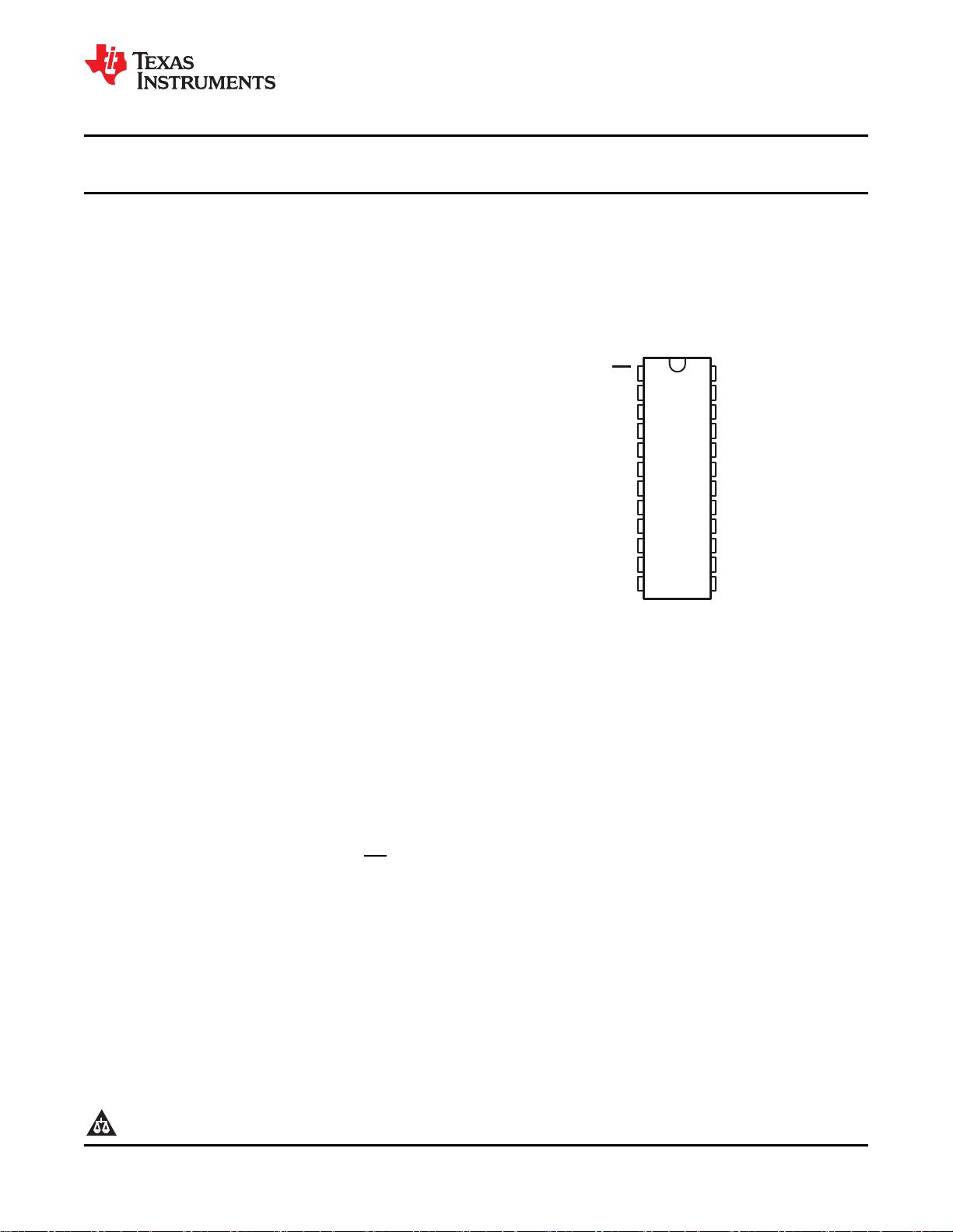
OE
AR
1R
2R
BR
AG
1G
2G
BG
AB
1B
GND
V
CC
BSCL
2SCL
1SCL
ASCL
BSCA
2SCA
1SCA
ASCA
BB
2B
SEL
1
2
3
4
5
6
7
8
9
10
11
12
24
23
22
21
20
19
18
17
16
15
14
13
TS5V522C
www.ti.com.cn
ZHCS156 –MARCH 2011
支持双通道
VGA 源极至汲极的 5 V、5 位视频交换开关 低导通电阻的 -2 V 下冲保护
查 询 样 品
: TS5V522C
1
特性
应用
• 双向数据流,支持近零传播延迟 • 数字及模拟信号接口
• 高带宽、380MHZ(典型值)RGB 开关 • 音频与视频信号接口
• 低导通阻抗 (ron) 特性(ron = 3 Ω 典型值) • 高速信号总线交换
• 低输入/输出电容可最大限度地减少加载与信号失 • 总线隔离与交错
真(CIO(OFF) = 8pF 典型值)
• 笔记本电脑图形控制
• 数据与控制输出上的下冲钳位二极管
• 低功耗(Icc = 3uA 最大值)
• Vcc 工作范围 4 V 至 5.5 V
• 数据 I/O 支持 0 至 5 V 信号级(0.8 V、1.2 V、1.5
V、1.8 V、2.5 V、3.3 V、4 V)
• 可在 I/O 上实施高达 5 V 的上拉电阻器
• I
off
支持带电插入、局部关断模式以及后驱动保护
• 闭锁性能超过 100 mA,符合 JESD 78 Class II 标
准
• ESD 性能等级超过 JESD 22 规范
– 2000 V 人体模型
(A114-B、Class II)
– 200 V 机器模型(A115-A)
– 1000 V 充电器件模型(C101)
说明
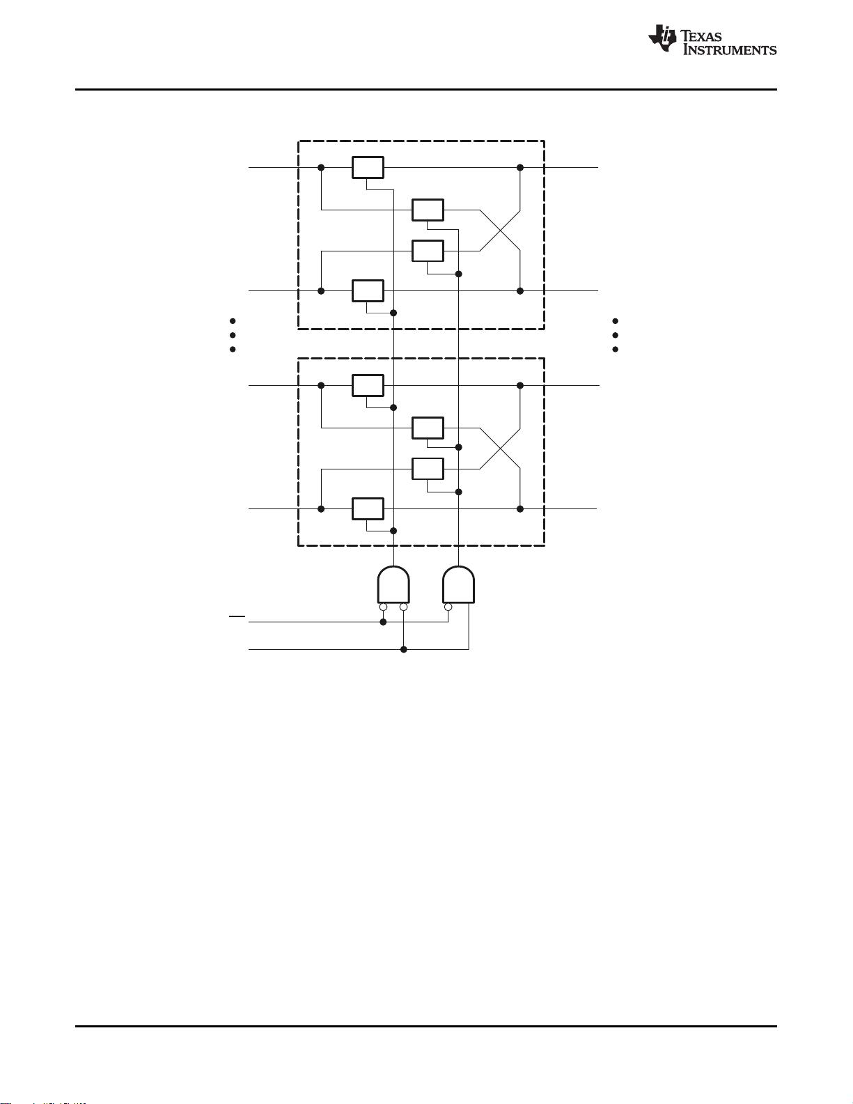
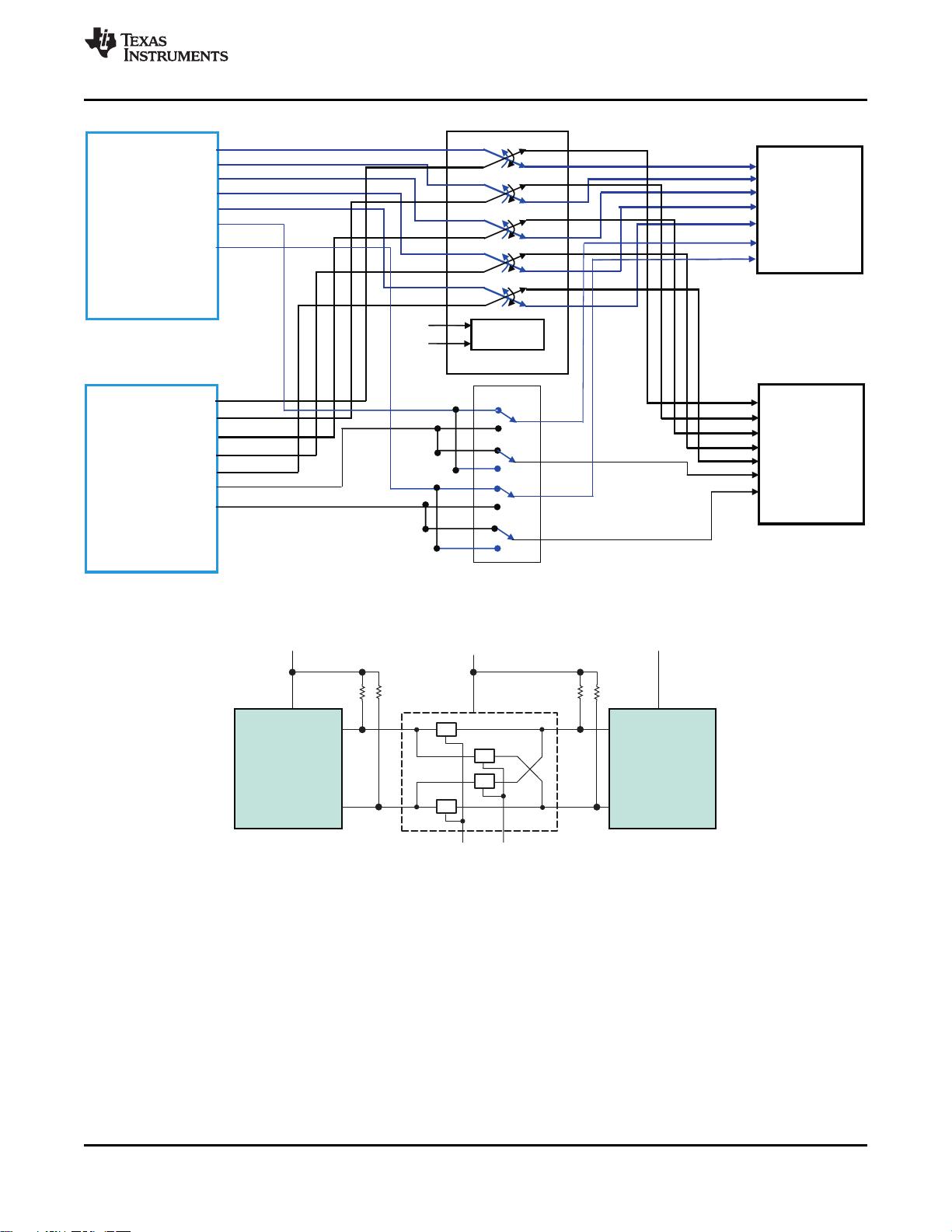
TS5V522C 是高带宽模拟开关,可为 VGA 信号开关提供 2:2 双图形交叉解决方案。 该器件支持 2 个 VGA 信号源
的开关,可在膝上型电脑中将信号指向两个目的位置中的一个。 TS5V522C 集成 5 个针对 RGB 信号的极高性能
380 Mhz(典型值)SPDT 开关、2 对适用于 HSYNC 与 VSYNC 线路的电平转换缓冲器以及集成型 ESD 保护。 5
个交叉开关均可通过 5 V 或 3.3 V TTL 控制信号控制。
TS5V522C 能够以更少的失真将 VGA 模拟信号带到目标位置。 DC 通道(SCA、SCL)可能需要 VGA 连接器上
+5 Vopen 的漏级,而且可能还需要在目标端上提供上拉电容器。 TS5V522C 数据端上的有源下冲保护电路可感测
下冲事件并确保在适当关闭状态下进行开关,从而可对低至 -2 V 的下冲事件提供保护。
要在上电或关断过程中确保高阻抗状态,OE 必须通过上拉电阻器的 V
CC
进行控制;驱动器电流吸收性能可检测电
阻器最小值。
1
Please be aware that an important notice concerning availability, standard warranty, and use in critical applications of Texas
Instruments semiconductor products and disclaimers thereto appears at the end of this data sheet.
PRODUCTION DATA information is current as of publication date.
Copyright © 2011, Texas Instruments Incorporated
Products conform to specifications per the terms of the Texas
Instruments standard warranty. Production processing does not English Data Sheet: SCDS317
necessarily include testing of all parameters.
剩余20页未读,继续阅读
资源评论


