Table of Contents
1 特性................................................................................... 1
2 应用................................................................................... 1
3 说明................................................................................... 1
4 Revision History.............................................................. 2
5 Description (continued).................................................. 2
6 Pin Configuration and Functions...................................3
7 Specifications.................................................................. 6
7.1 Absolute Maximum Ratings ....................................... 6
7.2 ESD Ratings .............................................................. 6
7.3 Recommended Operating Conditions ........................7
7.4 Thermal Information ...................................................7
7.5 Electrical Characteristics ............................................8
7.6 Typical Characteristics.............................................. 12
8 Detailed Description......................................................15
8.1 Overview................................................................... 15
8.2 Functional Block Diagram......................................... 16
8.3 Feature Description...................................................17
8.4 Device Functional Modes..........................................36
9 Application and Implementation.................................. 44
9.1 Application Information............................................. 44
9.2 Typical Application.................................................... 44
9.3 System Examples..................................................... 47
10 Power Supply Recommendations..............................50
11 Layout........................................................................... 51
11.1 Layout Guidelines................................................... 51
11.2 Layout Example...................................................... 52
12 Device and Documentation Support..........................53
12.1 Device Support....................................................... 53
12.2 Documentation Support.......................................... 53
12.3 接收文档更新通知................................................... 53
12.4 支持资源..................................................................53
12.5 Trademarks............................................................. 53
12.6 静电放电警告.......................................................... 53
12.7 术语表..................................................................... 53
13 Mechanical, Packaging, and Orderable
Information.................................................................... 54
4 Revision History
注:以前版本的页码可能与当前版本的页码不同
Changes from Revision * (October 2020) to Revision A (December 2020) Page
• 将器件状态从“预告信息”更改为“量产数据”................................................................................................ 1
5 Description (continued)
The input voltage range covers both of automotive cold-cranking and load dump scenarios. The switching
frequency is dynamically programmed in the range of 100 kHz to 2.2 MHz with an external resistor. Switching at
2.2 MHz minimizes AM band interference and allows for a small solution size and fast transient response.
The device features a low shutdown I
Q
and an ultra-low I
Q
sleep mode, which minimizes battery drain at no/light
load condition and eliminates the need for an additional low I
Q
LDO regulator as the CAN supply during standby.
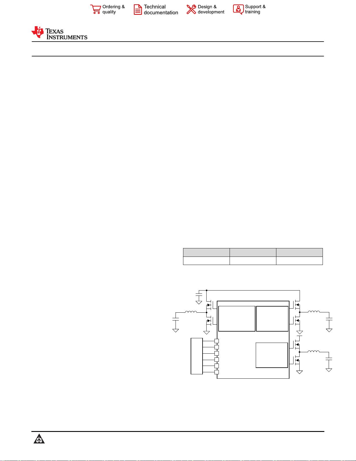
The device includes flexible topology channels that support boost or SEPIC, and two independent single-phase
bucks or a dual-phase buck to serve as a high current automotive processor supply. In boost mode, the device
supports bypass operation which eliminates the need for an external bypass switch. In buck mode, the device
supports low dropout operation to minimize dropout voltage. The battery monitor detects low battery voltage and
signals when a backup process should start.
Minimal power dissipation is realized with a low current limit threshold and the use of an external VCC supply.
The device has built-in protection features such as peak current limit which is constant over VIN, optional hiccup
mode overload protection, overvoltage protection, and thermal shutdown.
External clock synchronization, programmable spread spectrum switching frequency, as well as a leadless
package with minimal parasitics help to reduce EMI and avoid cross talk. Additional features include FPWM,
DCR sensing, programmable soft start, a precision reference, and power-good indicators.
LM5127-Q1
ZHCSMA4A – OCTOBER 2020 – REVISED DECEMBER 2020
www.ti.com.cn
2 Submit Document Feedback
Copyright © 2021 Texas Instruments Incorporated
Product Folder Links: LM5127-Q1


 信息提交成功


评论0
最新资源