没有合适的资源?快使用搜索试试~ 我知道了~
TI-TPS2206.pdf
需积分: 9 0 下载量 166 浏览量
2022-11-14
23:05:10
上传
评论 5
收藏 1.13MB PDF 举报
温馨提示
![preview](https://dl-preview.csdnimg.cn/87010671/0001-79e5435d5f228b47909eeccbd3c1947b_thumbnail.jpeg)
![preview-icon](https://csdnimg.cn/release/downloadcmsfe/public/img/scale.ab9e0183.png)
试读
33页
TI-TPS2206.pdf
资源推荐
资源详情
资源评论
![](https://csdnimg.cn/release/download_crawler_static/87010671/bg1.jpg)
SLVS138D − MAY 1996 − REVISED JANUARY 2001
1
POST OFFICE BOX 655303 • DALLAS, TEXAS 75265
D Fully Integrated V
CC
and V
pp
Switching for
Dual-Slot PC Card Interface
D P
2
C 3-Lead Serial Interface Compatible With
CardBus Controllers
D 3.3 V Low-Voltage Mode
D Meets PC Card Standards
D RESET for System Initialization of PC Cards
D 12-V Supply Can Be Disabled Except During
12-V Flash Programming
D Short Circuit and Thermal Protection
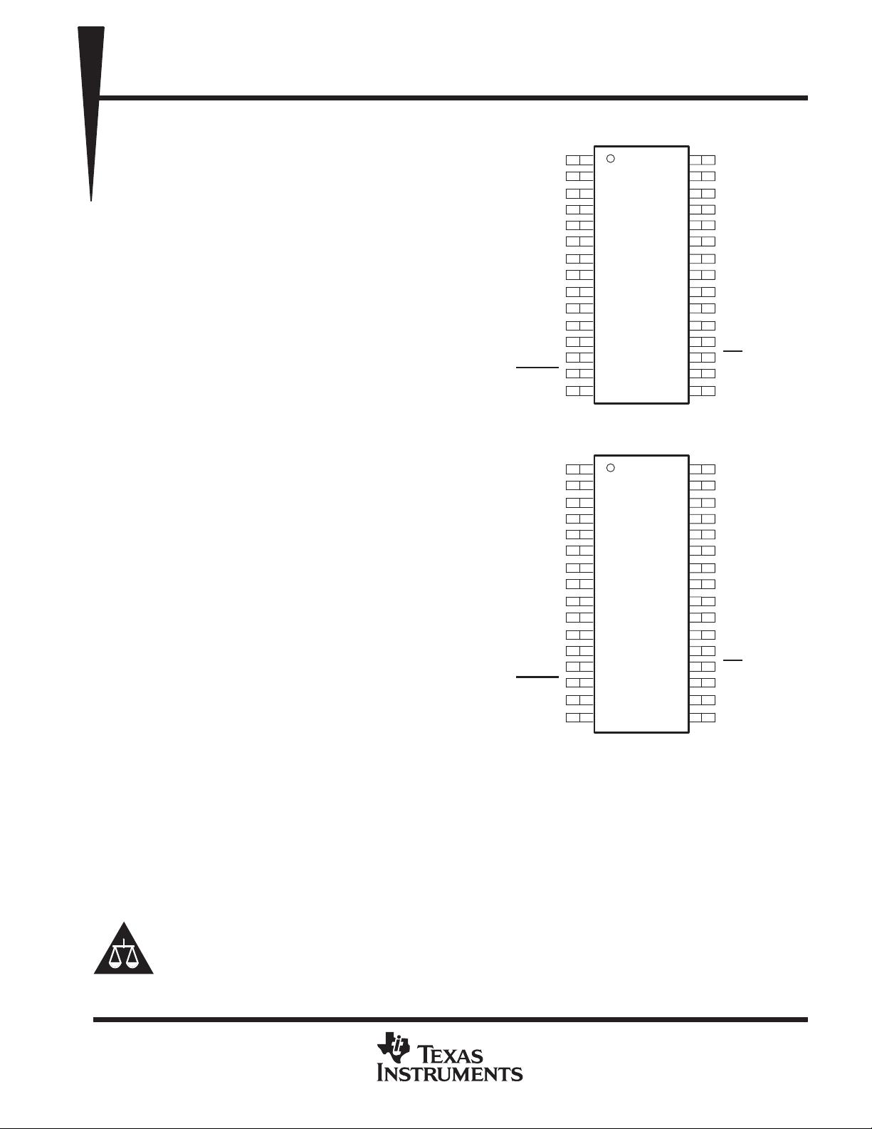
D 30-Pin SSOP (DB) and 32-Pin TSSOP (DAP)
D Compatible With 3.3-V, 5-V and 12-V PC Cards
D Low r
DS(on)
(140-mΩ 5-V V
CC
Switch; 110-mΩ
3.3-V V
CC
Switch)
D Break-Before-Make Switching
description
The TPS2206 PC Card power-interface switch
provides an integrated power-management solution
for two PC Cards. All of the discrete power
MOSFETs, a logic section, current limiting, and
thermal protection for PC Card control are
combined on a single integrated circuit (IC), using
the Texas Instruments LinBiCMOS process.
The circuit allows the distribution of 3.3-V, 5-V,
and/or 12-V card power by means of the P
2
C
(PCMCIA Peripheral-Control) Texas Instruments
nonproprietary serial interface. The current-limiting
feature eliminates the need for fuses, which
reduces component count and improves reliability.
The TPS2206 is backward compatible with the
TPS2202 and TPS2202A, except that there is no
V
DD
connection. Bias current is derived from
either the 3.3-V input pin or the 5-V input pin. The
TPS2206 also eliminates the APWR_GOOD and
BPWR_GOOD pins of the TPS2202 and
TPS2202A.
The TPS2206 features a 3.3-V low-voltage mode that allows for 3.3-V switching without the need for 5 V. This
facilitates low-power system designs such as sleep mode and pager mode where only 3.3 V is available.
Please be aware that an important notice concerning availability, standard warranty, and use in critical applications o
f
Texas Instruments semiconductor products and disclaimers thereto appears at the end of this data sheet.
LinBiCMOS and P
2
C are trademarks of Texas Instruments.
PC Card and CardBus are trademarks of PCMCIA (Personal Computer Memory Card International Association).
!" #!$% &"'
&! #" #" (" " ") !"
&& *+' &! #", &" ""%+ %!&"
", %% #""'
Copyright 2001, Texas Instruments Incorporated
1
2
3
4
5
6
7
8
9
10
11
12
13
14
15
30
29
28
27
26
25
24
23
22
21
20
19
18
17
16
5V
5V
DATA
CLOCK
LATCH
RESET
12V
AVPP
AVCC
AVCC
AVCC
GND
NC
RESET
3.3V
5V
NC
NC
NC
NC
NC
12V
BVPP
BVCC
BVCC
BVCC
NC
OC
3.3V
3.3V
DB OR DF PACKAGE
(TOP VIEW)
NC − No internal connection
1
2
3
4
5
6
7
8
9
10
11
12
13
14
15
16
32
31
30
29
28
27
26
25
24
23
22
21
20
19
18
17
5V
5V
NC
DATA
CLOCK
LATCH
RESET
12V
AVPP
AVCC
AVCC
AVCC
GND
RESET
NC
3.3V
5V
NC
NC
NC
NC
NC
NC
12V
BVPP
BVCC
BVCC
BVCC
OC
NC
3.3V
3.3V
DAP PACKAGE
(TOP VIEW)
![](https://csdnimg.cn/release/download_crawler_static/87010671/bg2.jpg)
SLVS138D − MAY 1996 − REVISED JANUARY 2001
2
POST OFFICE BOX 655303 • DALLAS, TEXAS 75265
description (continued)
The TPS2206 incorporates a reset function, selectable by one of two inputs, to help alleviate system errors. The
reset function enables PC Card initialization concurrent with host platform initialization, allowing a system reset.
Reset is accomplished by grounding the V
CC
and V
pp
(flash-memory programming voltage) outputs, which
discharges residual card voltage.
End equipment for the TPS2206 includes notebook computers, desktop computers, personal digital assistants
(PDAs), digital cameras and bar-code scanners.
AVAILABLE OPTIONS
T
A
PACKAGED DEVICES
CHIP FORM (Y)
T
A
PLASTIC SMALL OUTLINE (DB) PLASTIC SMALL OUTLINE (DF) TSSOP (DAP)
CHIP FORM (Y)
−40°C to 85°C TPS2206IDB TPS2206IDFR TPS2206IDAPR TPS2206Y
The DB package is available taped and reeled (add an R suffix to the device type, e.g., TPS2206IDBR). The DF and DAP packages are only
available taped and reeled, indicated by the R suffix.
typical PC card power-distribution application
PCMCIA
Controller
12 V
Power Supply
V
pp1
V
pp2
V
CC
V
CC
PC
Card A
TPS2206
5 V
3.3 V
OC
Serial Interface
3
V
pp1
V
pp2
V
CC
V
CC
PC
Card B
12V
5V
3.3V
AVPP
AVCC
AVCC
BVPP
BVCC
BVCC
BVCC
AVCC
Supervisor
RESET
RESET
![](https://csdnimg.cn/release/download_crawler_static/87010671/bg3.jpg)
SLVS138D − MAY 1996 − REVISED JANUARY 2001
3
POST OFFICE BOX 655303 • DALLAS, TEXAS 75265
TPS2206Y chip information
This chip, when properly assembled, displays characteristics similar to those of the TPS2206. Thermal
compression or ultrasonic bonding may be used on the doped-aluminum bonding pads. The chips may be
mounted with conductive epoxy or a gold-silicon preform.
BONDING PAD ASSIGNMENTS
CHIP THICKNESS: 15 TYPICAL
BONDING PADS: 4 × 4 MINIMUM
T
J
max = 150°C
TOLERANCES ARE ±10%.
ALL DIMENSIONS ARE IN MILS.
142
144
43
2
1
23
22
21
20
19
18
171614
15
13
12
11
10
9
8
7
6
5
TPS2206Y
5V
5V
DATA
CLOCK
LATCH
RESET
12V
AVPP
AVCC
AVCC
AVCC
GND
5V
12V
BVPP
BVCC
BVCC
BVCC
1
2
3
4
5
6
7
8
9
10
11
12
23
22
21
20
19
18
17
16
15
14
13
OC
3.3V
3.3V
3.3V
RESET
![](https://csdnimg.cn/release/download_crawler_static/87010671/bg4.jpg)
SLVS138D − MAY 1996 − REVISED JANUARY 2001
4
POST OFFICE BOX 655303 • DALLAS, TEXAS 75265
Terminal Functions
TERMINAL
NAME
NO.
I/O DESCRIPTION
NAME
DB, DF DAP
I/O
DESCRIPTION
3.3V 15, 16, 17 16, 17, 18 I 3.3-V V
CC
input for card power
5V 1, 2, 30 1, 2, 32 I 5-V V
CC
input for card power and/or chip power
12V 7, 24 8, 25 I 12-V V
pp
input for card power
AVCC 9, 10, 11 10, 11, 12 O Switched output that delivers 0 V, 3.3 V, 5 V, or high impedance to card
AVPP 8 9 O Switched output that delivers 0 V, 3.3 V, 5 V, 12 V, or high impedance to card
BVCC 20, 21, 22 21, 22, 23 O Switched output that delivers 0 V, 3.3 V, 5 V, or high impedance
BVPP 23 24 O Switched output that delivers 0 V, 3.3 V, 5 V, 12 V, or high impedance
CLOCK 4 5 I Logic-level clock for serial data word
DATA 3 4 I Logic-level serial data word
GND 12 13 Ground
LATCH 5 6 I Logic-level latch for serial data word
NC 13, 19, 25,
26, 27,
28, 29
3, 19, 26,
27, 28, 29,
30, 31
No internal connection
OC 18 20 O Logic-level overcurrent. OC reports output that goes low when an overcurrent condition exists
RESET 6 7 I Logic-level RESET input active high. Do not connect if terminal 14 is used.
RESET 14 14 I Logic-level RESET input active low. Do not connect if terminal 6 is used.
absolute maximum ratings over operating free-air temperature (unless otherwise noted)
†
Input voltage range for card power: V
I(5V)
−0.3 V to 7 V. . . . . . . . . . . . . . . . . . . . . . . . . . . . . . . . . . . . . . . . . . . .
V
I(3.3V)
−0.3 V to 7 V. . . . . . . . . . . . . . . . . . . . . . . . . . . . . . . . . . . . . . . . . . .
V
I(12V)
−0.3 V to 14 V. . . . . . . . . . . . . . . . . . . . . . . . . . . . . . . . . . . . . . . . . .
Logic input voltage −0.3 V to 7 V. . . . . . . . . . . . . . . . . . . . . . . . . . . . . . . . . . . . . . . . . . . . . . . . . . . . . . . . . . . . . . . . .
Continuous total power dissipation See Dissipation Rating Table. . . . . . . . . . . . . . . . . . . . . . . . . . . . . . . . . . . . .
Output current (each card): I
O(xVCC)
internally limited. . . . . . . . . . . . . . . . . . . . . . . . . . . . . . . . . . . . . . . . . . . . . . .
I
O(xVPP)
internally limited. . . . . . . . . . . . . . . . . . . . . . . . . . . . . . . . . . . . . . . . . . . . . . .
Operating virtual junction temperature range, T
J
−40°C to 150°C. . . . . . . . . . . . . . . . . . . . . . . . . . . . . . . . . . . . .
Operating free-air temperature range, T
A
−40°C to 85°C. . . . . . . . . . . . . . . . . . . . . . . . . . . . . . . . . . . . . . . . . . . .
Storage temperature range, T
stg
−55°C to 150°C. . . . . . . . . . . . . . . . . . . . . . . . . . . . . . . . . . . . . . . . . . . . . . . . . . .
Lead temperature 1,6 mm (1/16 inch) from case for 10 seconds 260°C. . . . . . . . . . . . . . . . . . . . . . . . . . . . . . .
†
Stresses beyond those listed under “absolute maximum ratings” may cause permanent damage to the device. These are stress ratings only, and
functional operation of the device at these or any other conditions beyond those indicated under “recommended operating conditions” is not
implied. Exposure to absolute-maximum-rated conditions for extended periods may affect device reliability.
DISSIPATION RATING TABLE
PACKAGE
T
A
≤ 25°C
POWER RATING
DERATING FACTOR
‡
ABOVE T
A
= 25°C
T
A
= 70°C
POWER RATING
T
A
= 85°C
POWER RATING
DB 1024 mW 8.2 mW/°C 655 mW 532 mW
DF 1158 mW 9.26 mW/°C 741 mW 602 mW
DAP
No backplane 1625 mW 13 mW/°C 1040 mW 845 mW
DAP
Backplane
§
6044 mW 48.36 mW/°C 3869 mW 3143 mW
‡
These devices are mounted on an FR4 board with no special thermal considerations.
§
2-oz backplane with 2-oz traces; 5.2-mm × 11-mm thermal pad with 6-mil solder; 0.18-mm diameter vias in a 3×6 array.
![](https://csdnimg.cn/release/download_crawler_static/87010671/bg5.jpg)
SLVS138D − MAY 1996 − REVISED JANUARY 2001
5
POST OFFICE BOX 655303 • DALLAS, TEXAS 75265
recommended operating conditions
MIN MAX UNIT
V
I(5V)
0 5.25 V
Input voltage range, V
I
V
I(3.3V)
0 5.25 V
Input voltage range, V
I
V
I(12V)
0 13.5 V
Output current
I
O(xVCC)
at 25°C 1 A
Output current
I
O(xVPP)
at 25°C 150 mA
Clock frequency 0 2.5 MHz
Operating virtual junction temperature, T
J
−40 125 °C
electrical characteristics, T
A
= 25°C, V
I(5V)
= 5 V (unless otherwise noted)
dc characteristics
PARAMETER
TEST CONDITIONS
TPS2206
UNIT
PARAMETER
TEST CONDITIONS
MIN TYP MAX
UNIT
5 V to xVCC 103 140
3.3 V to xVCC V
I(5V)
= 5 V, V
I(3.3
V)
= 3.3 V 69 110
mΩ
Switch resistances
†
3.3 V to xVCC V
I(5V)
= 0, V
I(3.3V)
= 3.3 V 96 180
mΩ
Switch resistances
†
5 V to xVPP 6
3.3 V to xVPP 6
Ω
12 V to xVPP 1
Ω
V
O(xVPP)
Clamp low voltage I
pp
at 10 mA 0.8 V
V
O(xVCC)
Clamp low voltage I
CC
at 10 mA 0.8 V
I
pp
high-impedance state
T
A
= 25°C 1 10
I
lkg
Leakage current
I
pp
high-impedance state
T
A
= 85°C 50
A
I
lkg
Leakage current
I
CC
high-impedance state
T
A
= 25°C 1 10
µA
I
CC
high-impedance state
T
A
= 85°C 50
V
I(5V)
= 5 V
V
O(AVCC)
= V
O(BVCC)
= 5 V,
V
O(AVPP)
= V
O(BVPP)
= 12 V
117 150
A
I
I
Input current
V
I(5V)
= 0,
V
I(3.3V)
= 3.3 V
V
O(AVCC)
= V
O(BVCC)
= 3.3 V,
V
O(AVPP)
= V
O(BVPP)
= 0
131 150
µA
Shutdown mode
V
O(BVCC)
= V
O(AVCC)
= V
O(AVPP)
= V
O(BVPP)
= Hi-Z
1 µA
I
OS
Short-circuit
I
O(xVCC)
T
J
= 85
°
C,
1 2.2 A
I
OS
Short-circuit
output-current limit
I
O(xVPP)
T
J
= 85 C,
Output powered up into a short to GND
120 400 mA
†
Pulse-testing techniques are used to maintain junction temperature close to ambient temperature; thermal effects must be taken into account
separately.
logic section
PARAMETER
TEST CONDITIONS
TPS2206
UNIT
PARAMETER
TEST CONDITIONS
MIN MAX
UNIT
Logic input current 1 µA
Logic input high level 2 V
Logic input low level 0.8 V
V
I(5V)
= 5 V,
I
O
= 1mA V
I(5V)
−0.4
Logic output high level
V
I(5V)
= 0,
V
I(3.3V)
= 3.3 V
I
O
= 1mA,
V
I(3.3V)
−0.4
V
Logic output low level I
O
= 1mA 0.4 V
剩余32页未读,继续阅读
资源评论
![avatar-default](https://csdnimg.cn/release/downloadcmsfe/public/img/lazyLogo2.1882d7f4.png)
![avatar](https://profile-avatar.csdnimg.cn/107303f5121d47e49d12d0a9ae68af10_weixin_54787054.jpg!1)
不觉明了
- 粉丝: 3250
- 资源: 5614
上传资源 快速赚钱
我的内容管理 展开
我的资源 快来上传第一个资源
我的收益
登录查看自己的收益我的积分 登录查看自己的积分
我的C币 登录后查看C币余额
我的收藏
我的下载
下载帮助
![voice](https://csdnimg.cn/release/downloadcmsfe/public/img/voice.245cc511.png)
![center-task](https://csdnimg.cn/release/downloadcmsfe/public/img/center-task.c2eda91a.png)
安全验证
文档复制为VIP权益,开通VIP直接复制
![dialog-icon](https://csdnimg.cn/release/downloadcmsfe/public/img/green-success.6a4acb44.png)