TI-TPS25740B.pdf
需积分: 9 39 浏览量
2022-10-29
00:07:19
上传
评论 6
收藏 2.45MB PDF 举报

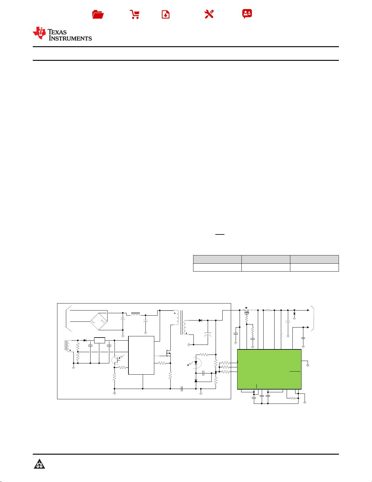
DRV
V
DD
CS
FB
UCC24636
T1
From AC Mains
TL431
+
²
P
P
P
HV
GND
LDO
VS
P
UCC28740
T1
TPS25740B
VDD
CC2
AGND
DVDD
CC1
DSCG
VTX
GND
GDNG
GDNS
CTL2
CTL1
Type-C
Plug
V
BUS
VPWR
HIPWR
PCTRL
GD
PSEL
VAUX
VBUS
ISNS
ENSRC
CSD17579Q3A
Power Supply
Copyright © 2016, Texas Instruments Incorporated
CTL3
Product
Folder
Order
Now
Technical
Documents
Tools &
Software
Support &
Community
An IMPORTANT NOTICE at the end of this data sheet addresses availability, warranty, changes, use in safety-critical applications,
intellectual property matters and other important disclaimers. PRODUCTION DATA.
English Data Sheet: SLVSDR6
TPS25740B
ZHCSGV1A –JUNE 2017–REVISED SEPTEMBER 2017
TPS25740B USB Type-C™ 和和 USB PD 源源控控制制器器
1
1 特特性性
1
• 通过 USB PD 2.0 认证(TID 编号 1030004)并符
合 USB PD 3.0 标准的供电器件
• 可通过引脚选择传输电压
– 5V、9V、12V 和 15V
– 5V、9V、15V 和 20V
• 可通过引脚选择峰值功率设置
– 8 个选项,取值范围为 18W 至 100W
• 高电压和安全功能集成
– 过压、过流、过热保护以及 V
BUS
放电
– CC1 和 CC2 上具有 IEC 61000-4-2 保护
– 故障状态下快速关断的输入引脚
– 外部 N 沟道 MOSFET 控制
– 3 引脚外部电源控制
– 宽 VIN 电源 (4.65V – 25V)
• 断开时的静态电流低于 10µA
• 端口连接指示器
• 用于双端口应用的自定向端口电源管理 功能
2 应应用用
• USB-PD 适配器(数据较少)
• 专用充电端口(数据较少)
• 电源集线器(数据较少)
• 移动电源
• 点烟器适配器 (CLA)
3 说说明明
无需任何固件配置,TPS25740B 即可实现通过 USB
电力输送 2.0 版本 1.2 认证和 Type-C™修订版 1.2 认
证的发送器,旨在最大限度缩短上市时间。根据设计,
该器件可与任何符合 USB PD 3.0 标准的接收器无缝
协作。该器件可通过监控 CC 引脚来检测是否有 USB
Type-C 接收器接入,然后通过启用 N 沟道 MOSFET
栅极驱动器来接通 VBUS。该器件随后使用 USB 电力
输送技术提供四种不同的电压。该器件使用三个输入引
脚(PSEL、HIPWR 和 PCTRL)来配置传输的电压和
电流。该器件会根据接入接收器的电压请求,使用
CTL1、CTL2 和 CTL3 引脚选择所需的电源电压。该
器件会按照 USB PD 要求自动使 VBUS 输出放电。
未连接设备时,TPS25740B 的流耗通常为
8.5µA(VDD = 3.3V 时为 5.8µA)。此外,还可以在
未连接设备时通过端口连接指示器 (DVDD) 输出来禁
用电源,从而节省更多的系统功耗。
保护 特性 包括过压保护、过流保护、过热保护、CC
引脚上的 IEC 保护以及用于禁用栅极驱动器的系统重
写引脚 (GD)。
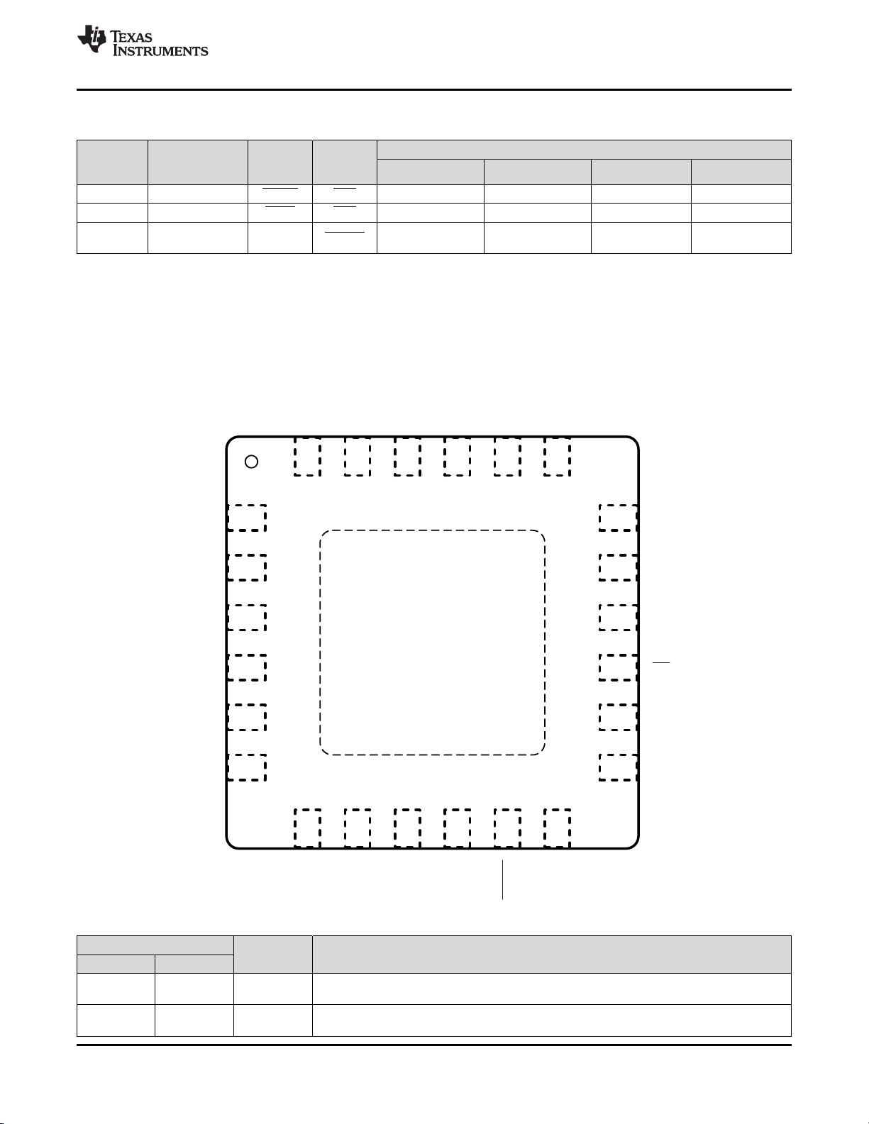
器器件件信信息息
(1)
器器件件型型号号 封封装装 封封装装尺尺寸寸((标标称称值值))
TPS25740B VQFN (24) 4.00mm x 4.00mm
(1) 如需了解所有可用封装,请参阅数据表末尾的可订购产品附
录。
简简化化电电路路原原理理图图
剩余65页未读,继续阅读
资源评论


不觉明了
- 粉丝: 3234
- 资源: 5614


最新资源
- 数据库管理工具:dbeaver-ce-23.0.3-stable.x86-64.rpm
- 外部中断0计数数码管显示0-9.zip
- xp系统安装.net框架包括镜像和.net4.0安装包
- c语言连接两个字符串.pdf
- 数据库管理工具:dbeaver-ce-23.0.3-macos-x86-64.dmg
- 数据库管理工具:dbeaver-ce-23.0.3-macos-aarch64.dmg
- Delphi 12 控件之DEV自动安装程序.exe
- 数据库管理工具:dbeaver-ce-23.0.2-x86-64-setup.exe
- Delphi 12 控件之AnySQL-0.0.9.rar
- 俄罗斯引擎Yandex的进入.pdf
资源上传下载、课程学习等过程中有任何疑问或建议,欢迎提出宝贵意见哦~我们会及时处理!
点击此处反馈


