瑞萨R7F0C903_908芯片资料
需积分: 5 169 浏览量
2022-05-05
10:29:59
上传
评论
收藏 1.64MB PDF 举报


Datasheet
R7F0C903-908
RENESAS MCU
True Low Power Platform (as low as 66 µA/MHz, and 0.57 µA for LVD), 1.6 V to 5.5 V
operation, 16 to 48 Kbyte Flash, 31 DMIPS at 24 MHz, for General Purpose Applications
Page 1 of 96
R01DS0237EJ0100
Rev.1.00
Jun 05, 2014
R01DS0237EJ0100 Rev.1.00
Jun 05, 2014
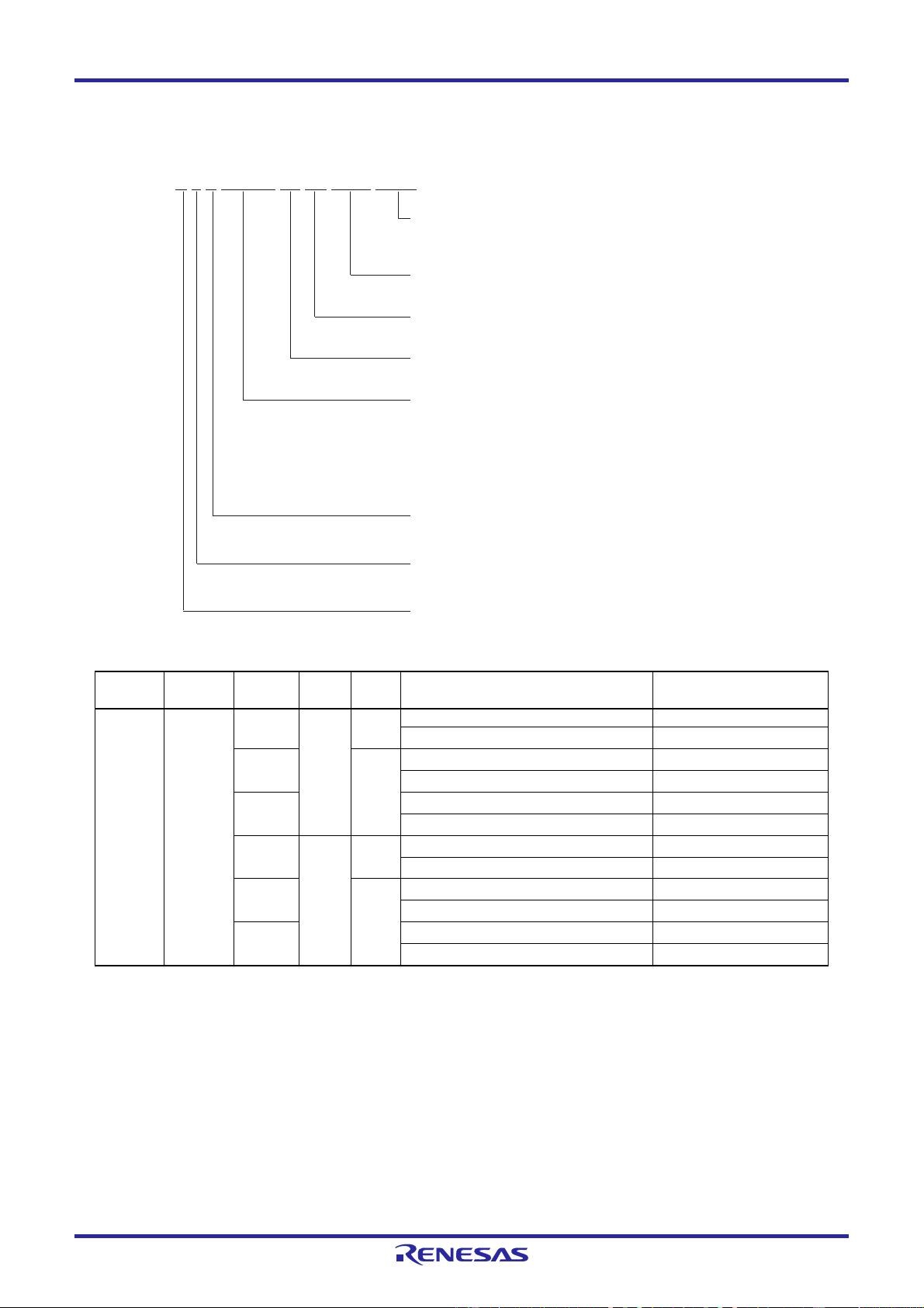
1. OUTLINE
1.1 Features
Ultra-Low Power Technology
1.6 V to 5.5 V operation from a single supply
Stop (RAM retained): 0.23 µA, (LVD enabled): 0.31
µA
Halt (LVD): 0.57 µA
Snooze: 0.70 mA (UART), 1.20 mA (ADC)
Operating: 66 µA/MHz
16-bit RL78 CPU Core
Delivers 31 DMIPS at maximum operating frequency
of 24 MHz
Instruction Execution: 86% of instructions can be
executed in 1 to 2 clock cycles
CISC Architecture (Harvard) with 3-stage pipeline
Multiply Signed & Unsigned: 16 x 16 to 32-bit result in
1 clock cycle
MAC: 16 x 16 to 32-bit result in 2 clock cycles
16-bit barrel shifter for shift & rotate in 1 clock cycle
1-wire on-chip debug function
Main Flash Memory
Density: 16 KB to 48 KB
Block size: 1 KB
On-chip single voltage flash memory with protection
from block erase/writing
Self-programming with secure boot swap function
and flash shield window function
Data Flash Memory
Data Flash with background operation
Data flash size: 2 KB size option or none
Erase Cycles: 1 Million (typ.)
Erase/programming voltage: 1.8 V to 5.5 V
RAM
2 KB or 3 KB size options
Supports operands or instructions
Back-up retention in all modes
High-speed On-chip Oscillator
24 MHz with +/ 1% accuracy over voltage (1.8 V to
5.5 V) and temperature (20 °C to 85 °C)
Pre-configured settings: 24 MHz, 16 MHz, 12 MHz, 8
MHz, 6 MHz, 4 MHz, 3 MHz, 2 MHz,
and 1 MHz
Reset and Supply Management
Power-on reset (POR) monitor/generator
Low voltage detection (LVD) with 14 setting options
(Interrupt and/or reset function)
Data Memory Access (DMA) Controller
2 channels
Transfer unit: 8- or 16-bit
Multiple Communication Interfaces
1 x I
2
C multi-master
Up to 3 x CSI/UART/Simple IIC
Extended-Function Timers
Multi-function 16-bit timers: Up to 8 channels
Interval Timer: 12-bit, 1 channel
15 kHz watchdog timer : 1 channel (window function)
Rich Analog
ADC: Up to 8 channels, 10-bit resolution, 2.1 µs
conversion time
Supports 1.6 V
Internal voltage reference (1.45 V)
Safety Features (IEC or UL 60730 compliance)
Flash memory CRC calculation
RAM parity error check
RAM write protection
SFR write protection
Illegal memory access detection
Clock stop/ frequency detection
ADC self-test
General Purpose I/O
5V tolerant, high-current (up to 20 mA per pin)
Open-Drain, Internal Pull-up support
Different potential interface support: Can connect to
a 1.8/2.5/3 V device
Operating Ambient Temperature
Standard: 40 °C to +85 °C
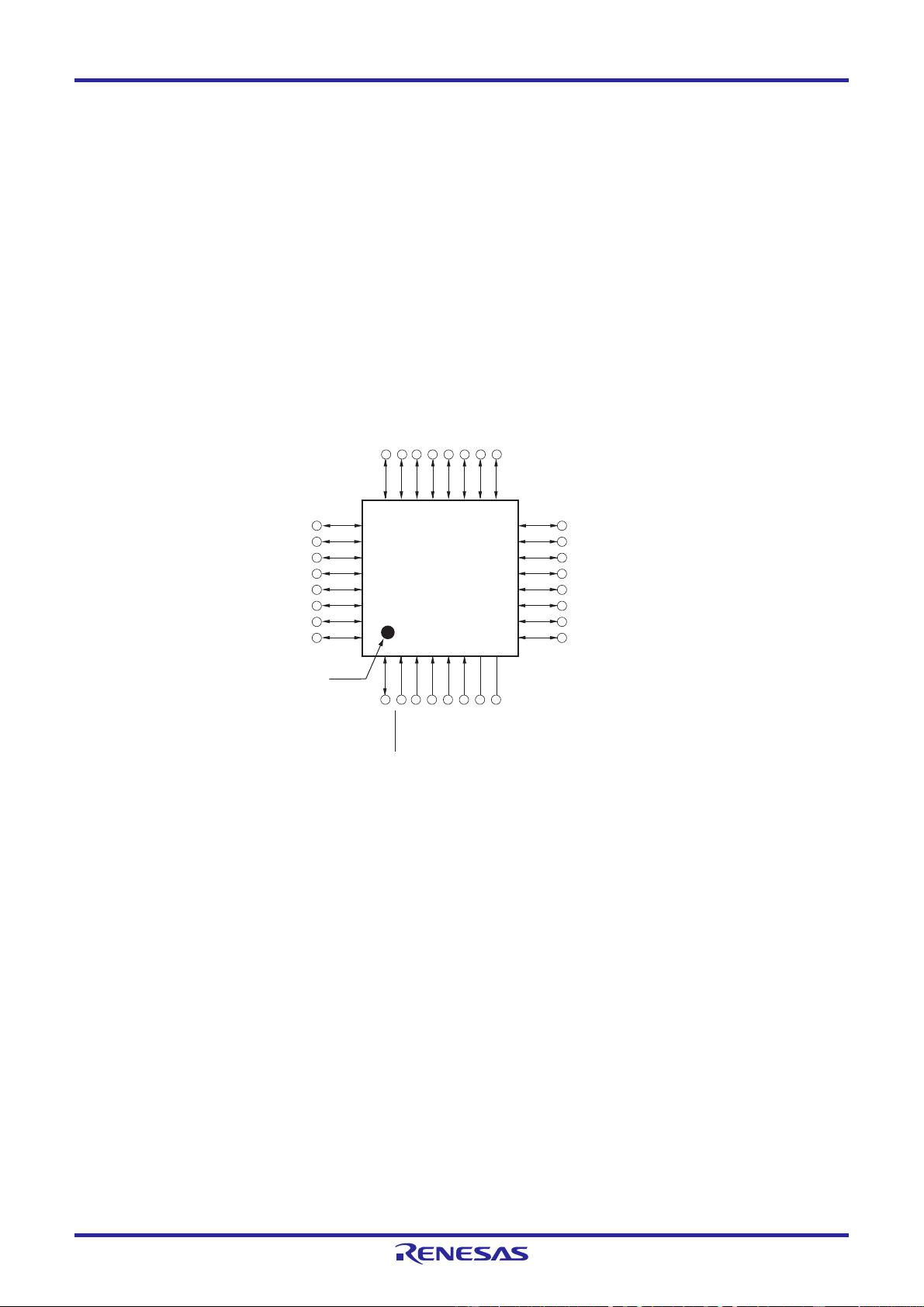
Package Type and Pin Count
32-pin LQFP (7 x 7 mm, 0.8 mm pitch)


剩余98页未读,继续阅读


评论0