


DDR2 SDRAM
MT47H256M4 – 32 Meg x 4 x 8 banks
MT47H128M8 – 16 Meg x 8 x 8 banks
MT47H64M16 – 8 Meg x 16 x 8 banks
Features
• V
DD
= 1.8V ±0.1V, V
DDQ
= 1.8V ±0.1V
• JEDEC-standard 1.8V I/O (SSTL_18-compatible)
• Differential data strobe (DQS, DQS#) option
• 4n-bit prefetch architecture
• Duplicate output strobe (RDQS) option for x8
• DLL to align DQ and DQS transitions with CK
• 8 internal banks for concurrent operation
• Programmable CAS latency (CL)
• Posted CAS additive latency (AL)
• WRITE latency = READ latency - 1
t
CK
• Selectable burst lengths (BL): 4 or 8
• Adjustable data-output drive strength
• 64ms, 8192-cycle refresh
• On-die termination (ODT)
• Industrial temperature (IT) option
• Automotive temperature (AT) option
• RoHS-compliant
• Supports JEDEC clock jitter specification
Options
1
Marking
• Configuration
– 256 Meg x 4 (32 Meg x 4 x 8 banks) 256M4
– 128 Meg x 8 (16 Meg x 8 x 8 banks) 128M8
– 64 Meg x 16 (8 Meg x 16 x 8 banks) 64M16
• FBGA package (Pb-free) – x16
– 84-ball FBGA (8mm x 12.5mm) Die
Rev :H
HR
– 84-ball FBGA (8mm x 12.5mm) Die
Rev :M
NF
• FBGA package (Pb-free) – x4, x8
– 60-ball FBGA (8mm x 10mm) Die
Rev :H
CF
– 60-ball FBGA (8mm x 10mm) Die
Rev :M
SH
• FBGA package (lead solder) – x16
– 84-ball FBGA (8mm x 12.5mm) Die
Rev :H
HW
• FBGA package (lead solder) – x4, x8
– 60-ball FBGA (8mm x 10mm) Die
Rev :H
JN
• Timing – cycle time
– 1.875ns @ CL = 7 (DDR2-1066) -187E
– 2.5ns @ CL = 5 (DDR2-800) -25E
– 3.0ns @ CL = 5 (DDR2-667) -3
• Self refresh
– Standard None
– Low-power L
• Operating temperature
– Commercial (0°C ≤ T
C
≤ +85°C)
2
None
– Industrial (–40°C ≤ T
C
≤ +95°C;
–40°C ≤ T
A
≤ +85°C)
IT
• Revision :H / :M
Notes:
1. Not all options listed can be combined to
define an offered product. Use the Part
Catalog Search on www.micron.com for
product offerings and availability.
2. For extended CT operating temperature see
IDD Table 11 (page 30) Note 7.
1Gb: x4, x8, x16 DDR2 SDRAM
Features
PDF: 09005aef8565148a
1GbDDR2.pdf – Rev. AA 07/14 EN
1
Micron Technology, Inc. reserves the right to change products or specifications without notice.
© 2007 Micron Technology, Inc. All rights reserved.
Products and specifications discussed herein are subject to change by Micron without notice.
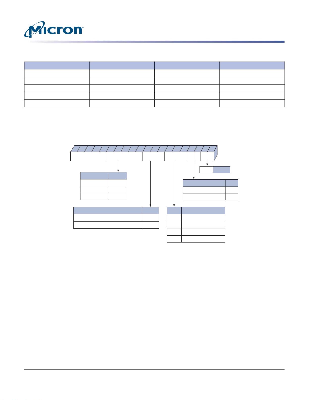
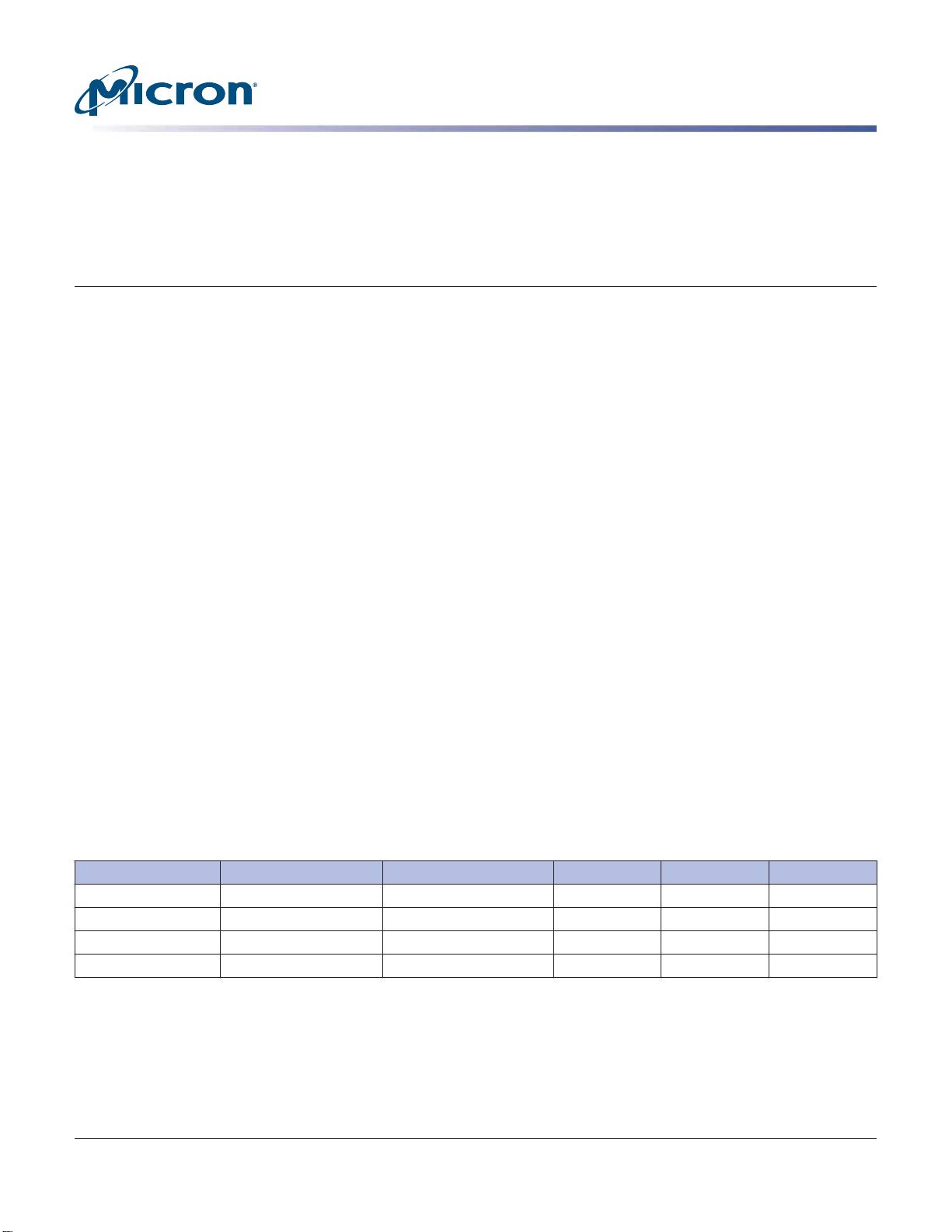
Table 1: Key Timing Parameters
Speed Grade
Data Rate (MT/s)
t
RC (ns)CL = 3 CL = 4 CL = 5 CL = 6 CL = 7
-187E 400 533 800 800 1066 54
-25E 400 533 800 800 n/a 55
-3 400 533 667 n/a n/a 55
Table 2: Addressing
Parameter 256 Meg x 4 128 Meg x 8 64 Meg x 16
Configuration 32 Meg x 4 x 8 banks 16 Meg x 8 x 8 banks 8 Meg x 16 x 8 banks
Refresh count 8K 8K 8K
Row address A[13:0] (16K) A[13:0] (16K) A[12:0] (8K)
Bank address BA[2:0] (8) BA[2:0] (8) BA[2:0] (8)
Column address A[11, 9:0] (2K) A[9:0] (1K) A[9:0] (1K)
Figure 1: 1Gb DDR2 Part Numbers
Package
Pb-free
84-ball 8mm x 12.5mm FBGA
60-ball 8mm x 10.0mm FBGA
60-ball 8mm x 10.0mm FBGA
Lead solder
84-ball 8mm x 12.5mm FBGA
60-ball 8mm x 10mm FBGA
HR
SH
CF
HW
JN
Example Part Number: MT47H128M8SH-25E:M
Configuration
256 Meg x 4
128 Meg x 8
64 Meg x 16
256M4
128M8
64M16
Speed Grade
t
CK = 1.875ns, CL = 7
t
CK = 2.5ns, CL = 5
t
CK = 3ns, CL = 5
-187E
-25E
-3
-
ConfigurationMT47H Package Speed
Revision
Revision
:H/:M
:
Low power
Industrial temperature
L
IT
{
84-ball 8mm x 12.5mm FBGA
NF
Note:
1. Not all speeds and configurations are available in all packages.
FBGA Part Number System
Due to space limitations, FBGA-packaged components have an abbreviated part marking that is different from the
part number. For a quick conversion of an FBGA code, see the FBGA Part Marking Decoder on Micron’s Web site:
http://www.micron.com.
1Gb: x4, x8, x16 DDR2 SDRAM
Features
PDF: 09005aef8565148a
1GbDDR2.pdf – Rev. AA 07/14 EN
2
Micron Technology, Inc. reserves the right to change products or specifications without notice.
© 2007 Micron Technology, Inc. All rights reserved.

Contents
State Diagram .................................................................................................................................................. 8
Functional Description ..................................................................................................................................... 9
Industrial Temperature ................................................................................................................................. 9
General Notes ............................................................................................................................................ 10
Functional Block Diagrams ............................................................................................................................. 11
Ball Assignments and Descriptions ................................................................................................................. 14
Packaging ...................................................................................................................................................... 18
Package Dimensions ................................................................................................................................... 18
FBGA Package Capacitance ......................................................................................................................... 22
Electrical Specifications – Absolute Ratings ..................................................................................................... 23
Temperature and Thermal Impedance ........................................................................................................ 23
Electrical Specifications – I
DD
Parameters ........................................................................................................ 26
I
DD
Specifications and Conditions ............................................................................................................... 26
I
DD7
Conditions .......................................................................................................................................... 27
AC Timing Operating Specifications ................................................................................................................ 32
AC and DC Operating Conditions .................................................................................................................... 44
ODT DC Electrical Characteristics ................................................................................................................... 44
Input Electrical Characteristics and Operating Conditions ............................................................................... 45
Output Electrical Characteristics and Operating Conditions ............................................................................. 48
Output Driver Characteristics ......................................................................................................................... 50
Power and Ground Clamp Characteristics ....................................................................................................... 54
AC Overshoot/Undershoot Specification ......................................................................................................... 55
Input Slew Rate Derating ................................................................................................................................ 57
Commands .................................................................................................................................................... 70
Truth Tables ............................................................................................................................................... 70
DESELECT ................................................................................................................................................. 74
NO OPERATION (NOP) ............................................................................................................................... 75
LOAD MODE (LM) ...................................................................................................................................... 75
ACTIVATE .................................................................................................................................................. 75
READ ......................................................................................................................................................... 75
WRITE ....................................................................................................................................................... 75
PRECHARGE .............................................................................................................................................. 76
REFRESH ................................................................................................................................................... 76
SELF REFRESH ........................................................................................................................................... 76
Mode Register (MR) ........................................................................................................................................ 76
Burst Length .............................................................................................................................................. 77
Burst Type .................................................................................................................................................. 78
Operating Mode ......................................................................................................................................... 78
DLL RESET ................................................................................................................................................. 78
Write Recovery ........................................................................................................................................... 79
Power-Down Mode ..................................................................................................................................... 79
CAS Latency (CL) ........................................................................................................................................ 80
Extended Mode Register (EMR) ....................................................................................................................... 81
DLL Enable/Disable ................................................................................................................................... 82
Output Drive Strength ................................................................................................................................ 82
DQS# Enable/Disable ................................................................................................................................. 82
RDQS Enable/Disable ................................................................................................................................. 82
Output Enable/Disable ............................................................................................................................... 82
On-Die Termination (ODT) ......................................................................................................................... 83
Off-Chip Driver (OCD) Impedance Calibration ............................................................................................ 83
1Gb: x4, x8, x16 DDR2 SDRAM
Features
PDF: 09005aef8565148a
1GbDDR2.pdf – Rev. AA 07/14 EN
3
Micron Technology, Inc. reserves the right to change products or specifications without notice.
© 2007 Micron Technology, Inc. All rights reserved.

Posted CAS Additive Latency (AL) ................................................................................................................ 83
Extended Mode Register 2 (EMR2) ................................................................................................................... 85
Extended Mode Register 3 (EMR3) ................................................................................................................... 86
Initialization .................................................................................................................................................. 87
ACTIVATE ...................................................................................................................................................... 90
READ ............................................................................................................................................................. 92
READ with Precharge .................................................................................................................................. 96
READ with Auto Precharge .......................................................................................................................... 98
WRITE .......................................................................................................................................................... 103
PRECHARGE ................................................................................................................................................. 113
REFRESH ...................................................................................................................................................... 114
SELF REFRESH .............................................................................................................................................. 115
Power-Down Mode ........................................................................................................................................ 117
Precharge Power-Down Clock Frequency Change ........................................................................................... 124
Reset ............................................................................................................................................................. 125
CKE Low Anytime ...................................................................................................................................... 125
ODT Timing .................................................................................................................................................. 127
MRS Command to ODT Update Delay ........................................................................................................ 129
1Gb: x4, x8, x16 DDR2 SDRAM
Features
PDF: 09005aef8565148a
1GbDDR2.pdf – Rev. AA 07/14 EN
4
Micron Technology, Inc. reserves the right to change products or specifications without notice.
© 2007 Micron Technology, Inc. All rights reserved.

List of Figures
Figure 1: 1Gb DDR2 Part Numbers ................................................................................................................... 2
Figure 2: Simplified State Diagram ................................................................................................................... 8
Figure 3: 256 Meg x 4 Functional Block Diagram ............................................................................................. 11
Figure 4: 128 Meg x 8 Functional Block Diagram ............................................................................................. 12
Figure 5: 64 Meg x 16 Functional Block Diagram ............................................................................................. 13
Figure 6: 60-Ball FBGA – x4, x8 Ball Assignments (Top View) ........................................................................... 14
Figure 7: 84-Ball FBGA – x16 Ball Assignments (Top View) ............................................................................... 15
Figure 8: 84-Ball FBGA Package (8mm x 12.5mm) – x16 Die Rev :H .................................................................. 18
Figure 9: 60-Ball FBGA (8mm x 10mm) – x4, x8 Die Rev :H ............................................................................... 19
Figure 10: 84-Ball FBGA Package (8mm x 12.5mm) – x16; "NF" Die Rev :M ....................................................... 20
Figure 11: 60-Ball FBGA (8mm x 10mm) – x4, x8; "SH" Die Rev :M ................................................................... 21
Figure 12: Example Temperature Test Point Location ...................................................................................... 24
Figure 13: Single-Ended Input Signal Levels ................................................................................................... 45
Figure 14: Differential Input Signal Levels ...................................................................................................... 46
Figure 15: Differential Output Signal Levels .................................................................................................... 48
Figure 16: Output Slew Rate Load .................................................................................................................. 49
Figure 17: Full Strength Pull-Down Characteristics ......................................................................................... 50
Figure 18: Full Strength Pull-Up Characteristics .............................................................................................. 51
Figure 19: Reduced Strength Pull-Down Characteristics .................................................................................. 52
Figure 20: Reduced Strength Pull-Up Characteristics ...................................................................................... 53
Figure 21: Input Clamp Characteristics .......................................................................................................... 54
Figure 22: Overshoot ..................................................................................................................................... 55
Figure 23: Undershoot ................................................................................................................................... 55
Figure 24: Nominal Slew Rate for
t
IS ............................................................................................................... 60
Figure 25: Tangent Line for
t
IS ........................................................................................................................ 60
Figure 26: Nominal Slew Rate for
t
IH .............................................................................................................. 61
Figure 27: Tangent Line for
t
IH ....................................................................................................................... 61
Figure 28: Nominal Slew Rate for
t
DS ............................................................................................................. 66
Figure 29: Tangent Line for
t
DS ...................................................................................................................... 66
Figure 30: Nominal Slew Rate for
t
DH ............................................................................................................. 67
Figure 31: Tangent Line for
t
DH ..................................................................................................................... 67
Figure 32: AC Input Test Signal Waveform Command/Address Balls ................................................................ 68
Figure 33: AC Input Test Signal Waveform for Data with DQS, DQS# (Differential) ............................................ 68
Figure 34: AC Input Test Signal Waveform for Data with DQS (Single-Ended) ................................................... 69
Figure 35: AC Input Test Signal Waveform (Differential) .................................................................................. 69
Figure 36: MR Definition ............................................................................................................................... 77
Figure 37: CL ................................................................................................................................................. 80
Figure 38: EMR Definition ............................................................................................................................. 81
Figure 39: READ Latency ............................................................................................................................... 84
Figure 40: WRITE Latency .............................................................................................................................. 84
Figure 41: EMR2 Definition ........................................................................................................................... 85
Figure 42: EMR3 Definition ........................................................................................................................... 86
Figure 43: DDR2 Power-Up and Initialization ................................................................................................. 87
Figure 44: Example: Meeting
t
RRD (MIN) and
t
RCD (MIN) .............................................................................. 90
Figure 45: Multibank Activate Restriction ....................................................................................................... 91
Figure 46: READ Latency ............................................................................................................................... 93
Figure 47: Consecutive READ Bursts .............................................................................................................. 94
Figure 48: Nonconsecutive READ Bursts ........................................................................................................ 95
Figure 49: READ Interrupted by READ ............................................................................................................ 96
Figure 50: READ-to-WRITE ............................................................................................................................ 96
1Gb: x4, x8, x16 DDR2 SDRAM
Features
PDF: 09005aef8565148a
1GbDDR2.pdf – Rev. AA 07/14 EN
5
Micron Technology, Inc. reserves the right to change products or specifications without notice.
© 2007 Micron Technology, Inc. All rights reserved.


