Chapter 1: SDRAM Controller Core 1–3
Functional Description
© March 2009 Altera Corporation Quartus II Handbook Version 9.0 Volume 5: Embedded Peripherals
Off-Chip SDRAM Interface
The interface to the external SDRAM chip presents the signals defined by the PC100
standard. These signals must be connected externally to the SDRAM chip(s) through
I/O pins on the Altera device.
Signal Timing and Electrical Characteristics
The timing and sequencing of signals depends on the configuration of the core. The
hardware designer configures the core to match the SDRAM chip chosen for the
system. See “Instantiating the Core in SOPC Builder” on page 1–5 for details. The
electrical characteristics of the device pins depend on both the target device family
and the assignments made in the Quartus
®
II software. Some device families support
a wider range of electrical standards, and therefore are capable of interfacing with a
greater variety of SDRAM chips. For details, refer to the device handbook for the
target device family.
Synchronizing Clock and Data Signals
The clock for the SDRAM chip (SDRAM clock) must be driven at the same frequency
as the clock for the Avalon-MM interface on the SDRAM controller (controller clock).
As in all synchronous designs, you must ensure that address, data, and control signals
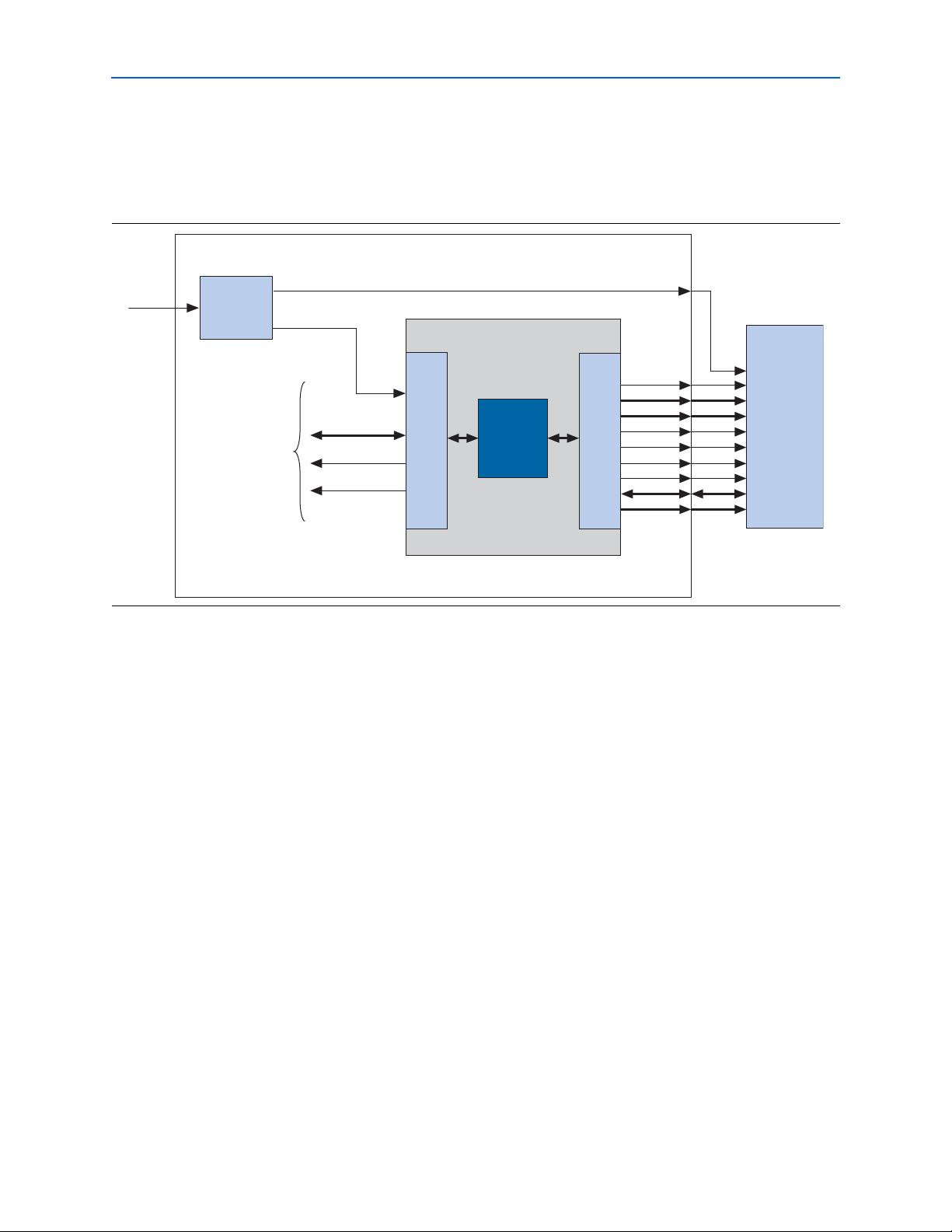
at the SDRAM pins are stable when a clock edge arrives. As shown in Figure 1–1, you
can use an on-chip phase-locked loop (PLL) to alleviate clock skew between the
SDRAM controller core and the SDRAM chip. At lower clock speeds, the PLL might
not be necessary. At higher clock rates, a PLL is necessary to ensure that the SDRAM
clock toggles only when signals are stable on the pins. The PLL block is not part of the
SDRAM controller core. If a PLL is necessary, you must instantiate it manually. You
can instantiate the PLL core interface, which is an SOPC Builder component, or
instantiate an ALTPLL megafunction outside the SOPC Builder system module.
If you use a PLL, you must tune the PLL to introduce a clock phase shift so that
SDRAM clock edges arrive after synchronous signals have stabilized. See “Clock, PLL
and Timing Considerations” on page 1–10 for details.
f For more information about instantiating a PLL in your SOPC Builder system, refer to
PLL Core chapter in volume 5 of the Quartus II Handbook. The Nios
®
II development
tools provide example hardware designs that use the SDRAM controller core in
conjunction with a PLL, which you can use as a reference for your custom designs.
The Nios II development tools are available free for download from www.altera.com.
Clock Enable (CKE) Not Supported
The SDRAM controller does not support clock-disable modes. The SDRAM controller
permanently asserts the CKE signal on the SDRAM.
Sharing Pins with Other Avalon-MM Tri-State Devices
If an Avalon-MM tri-state bridge is present in the SOPC Builder system, the SDRAM
controller core can share pins with the existing tri-state bridge. In this case, the core’s
addr, dq (data) and dqm (byte-enable) pins are shared with other devices connected
to the Avalon-MM tri-state bridge. This feature conserves I/O pins, which is valuable
in systems that have multiple external memory chips (for example, flash, SRAM, and
SDRAM), but too few pins to dedicate to the SDRAM chip. See “Performance
Considerations” for details about how pin sharing affects performance.


