ARM-JTAG Wiggler COMPATIBLE DONGLE
FOR PROGRAMMING AND DEBUGGING
Features:
• program LPC2000 family and other (tested
with OKI ML674000) ARM flash
microcontrollers
• uses ARM standard 2x10 pin JTAG
connector
• no need for external power supply, all power
is taken from the target board
• compatible with Rowley's CrossConnect,
IAR EWARM and GCC (OCD) software for
programming, real time emulation,
debugging, step by step program execution,
breakpoints, memory dump etc everything
all high priced emulators do
• dimensions 50x40 mm (2x1.6") + 20 cm
(8") cable
Supported devices:
Philips Semiconductors Inc . LPC2000 16/32-bit
ARM7TDMI-S™ family, OKI Semiconductors
ML6740016/32-bit ARM7 family.
It should work with all other ARM7 and ARM9
microcontrollers, but this is not tested.
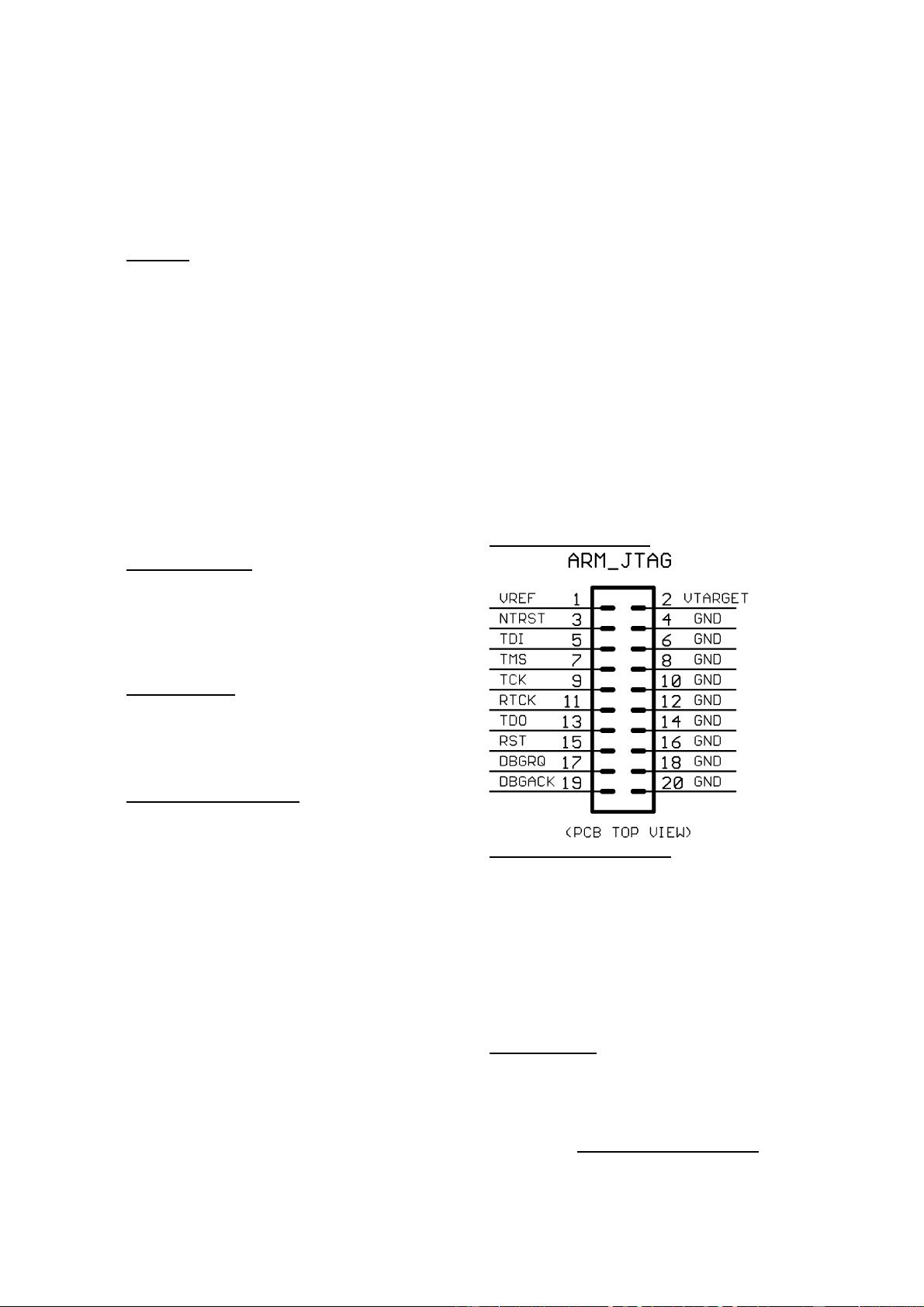
JTAG interface:
The JTAG connector is 2x10 pin with 0,1" step
and ARM recommended JTAG layout. PIN.1 is
marked with square pad on bottom and arrow on
top.
JTAG signals description:
PIN.1 (VTREF) Target voltage sense. Used to
indicate the target’s operating voltage to the
debug tool.
PIN.2 (VTARGET) Target voltage. May be
used to supply power to the debug tool.
PIN.3 (nTRST) JTAG TAP reset, this signal
should be pulled up to Vcc in target board.
PIN4,6, 8, 10,12,14,16,18,20 Ground. The Gnd-
Signal-Gnd-Signal strategy implemented on the
20-way connection scheme improves noise
immunity on the target connect cable.
PIN.5 (TDI) JTAG serial data in, should be
pulled up to Vcc on target board.
PIN.7 (TMS) JTAG TAP Mode Select, should
be pulled up to Vcc on target board.
PIN.9 (TCK) JTAG clock.
PIN.11 (RTCK) JTAG retimed clock.
Implemented on certain ASIC ARM
implementations the host ASIC may need to
synchronize external inputs (such as JTAG
inputs) with its own internal clock.
PIN.13 (TDO) JTAG serial data out.
PIN.15 (nSRST) Target system reset.
PIN.17 (DBGRQ) Asynchronous debug request.
DBGRQ allows an external signal to force the
ARM core into debug mode, should be pull
down to GND.
PIN.19 (DBGACK) Debug acknowledge. The
ARM core acknowledges debug-mode in
response to a DBGRQ input.
JTAG connector layout:
PCB design considerations:
Use single point to point connections between
ARM core and JTAG connector. The length of
all tracks must match to within 2-3 cm (1”).
JTAG connector should be placed as near Arm
core as possible. If lines are longer than 5 cm
(2”) they should be series terminated at device
end with series resistors equal to the
characteristic impedance of the PCB tracks and
the connector.
Ordering codes:
ARM-JTAG - assembled and tested
Copyright(c) 2004, OLIMEX Ltd., All rights reserved.
Development boards for ARM, AVR, MSP430 and PIC microcontrollers http://www.olimex.com/dev