没有合适的资源?快使用搜索试试~ 我知道了~
ON SEMI_NCS2632-D NOCAP:trade_mark:, Pop-Free,-综合文档
需积分: 5 0 下载量 29 浏览量
2021-05-25
06:47:07
上传
评论
收藏 204KB PDF 举报
温馨提示
试读
15页
ON SEMI_NCS2632-D NOCAP:trade_mark:, Pop-Free, 3 Vrms Audio Line Driver.PDF
资源详情
资源评论
资源推荐
© Semiconductor Components Industries, LLC, 2013
October, 2013 − Rev. 4
1 Publication Order Number:
NCS2632/D
NCS2632
NOCAP], Pop-Free, 3 V
RMS
Audio Line Driver with
Adjustable Gain
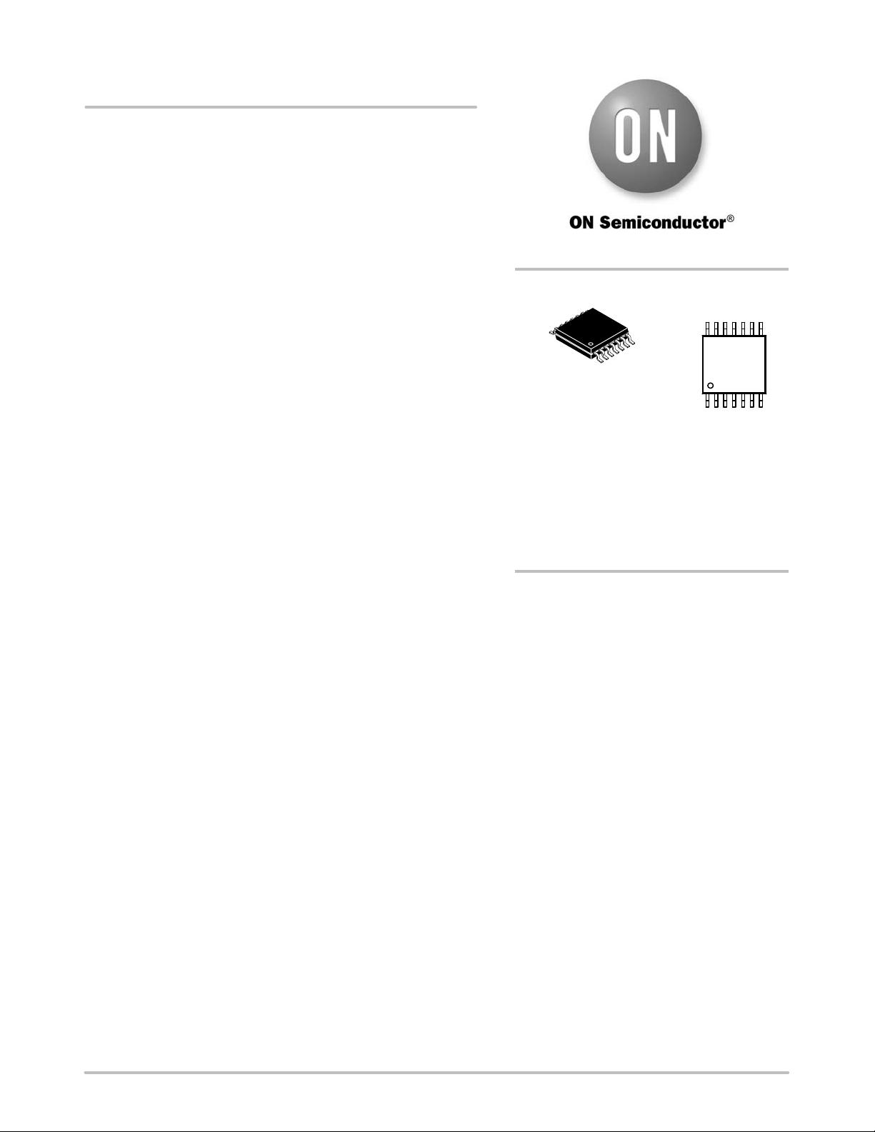
The NCS2632 is a pop−free stereo line driver. It uses
ON Semiconductor’s patented NOCAP technology which allows the
elimination of the external DC−blocking capacitors by providing
ground−referenced outputs through the generation of an internal
negative supply rail. The device can drive 3 V
RMS
into a 600 W load at
5 V power supply. By eliminating the two external heavy coupling
capacitors, the NOCAP approach offers significant space and cost
savings compared to similar audio solutions.
The NCS2632 has differential inputs and is available with an
external adjustable gain ranging from ±1 V/V to ±10 V/V. The gain is
adjusted with external resistors. The device can also be configured as a
2nd order low pass filter to complement DAC’s and SOC converters.
In addition to the NOCAP architecture, it contains specific circuitry to
prevent “Pop & Click” noise from occurring during Enable /
Shutdown transitions. The Signal-to-Noise Ratio reaches 105 dB,
offering high fidelity audio sound. The NCS2632 exhibits a high
power supply rejection with a typical value of 90 dB. This device also
features an Under−Voltage Protection (UVP) function which can be
adjusted using an external resistor bridge. The device is available in a
TSSOP−14 package.
Features
• NOCAP
♦ Eliminates Pop/Clicks
♦ Eliminates Output DC−Blocking Capacitors –
Provides Flat Frequency Response 20 Hz – 20 kHz
• Supply Voltage from 2.2 V to 5.5 V
• Low Noise and THD
♦ SNR = 105 dB
♦ Typical V
n
at 8 mVrms, A−Weighted
♦ THD+N < 0.001% at 1 kHz
• Output Voltage into 600 W Load
♦ 2 V
RMS
with 3.3 V Supply Voltage
♦ 3 V
RMS
with 5 V Supply Voltage
• Adjustable Gain from ± 1 V/V to ± 10 V/V
• Differential Input
• High PSRR: 90 dB
• External Under−Voltage Detection Function
• Enhanced Pop & Click Suppression Function
• Offset Voltage ≤ ±400 mV
• Outputs pass ±8 kV contact discharge according to
IEC61000−4−2 under application conditions
• Available in a TSSOP−14 package
• These Devices are Pb−Free, Halogen Free/BFR Free
and are RoHS Compliant
Applications
• Set−Top Boxes
• PDP / LCD TV
• Blu−ray™ Player, DVD Players
• Home Theater in a Box
• Laptops, Notebook PCs
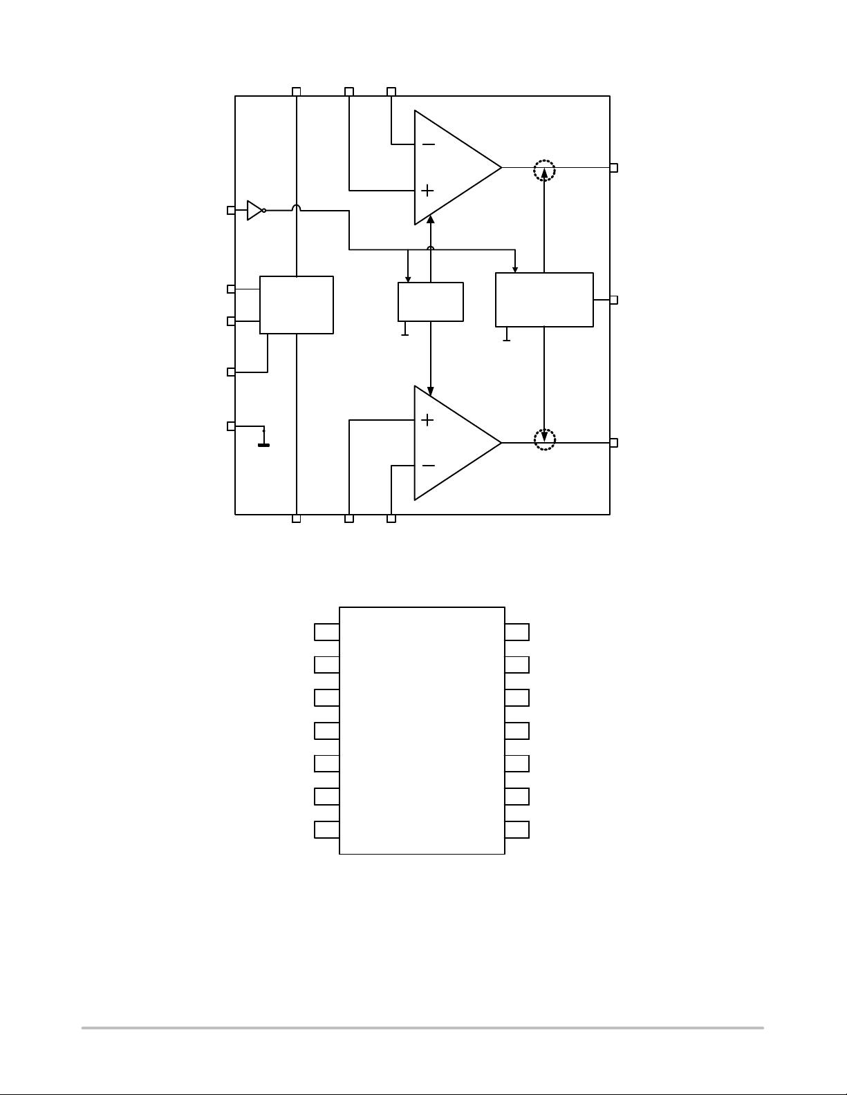
MARKING
DIAGRAM
http://onsemi.com
A = Assembly Location
L = Wafer Lot
Y = Year
W = Work Week
G = Pb−Free Package
1
14
TSSOP−14
CASE 948G
NCS
2632
ALYWG
G
1
14
See detailed ordering and shipping information in the package
dimensions section on page 13 of this data sheet.
ORDERING INFORMATION
*For additional marking information, refer to
Application Note AND8473/D.
(*Note: Microdot may be in either location)
NCS2632
http://onsemi.com
2
Charge
Pump
Circuitry
Click/Pop
Suppression
Circuitry
Bias
Circuitry
VDD INLP INLM
CP
CN
OUTL
OUTR
VSS INRMINRP
PGND
AGND
EN
AGND
AGND
UVP
Figure 1. NCS2632, Simplified Block Diagram
1
2
3
4
5
6
7
14
13
12
11
10
9
8
INRP
INRM
OUTR
AGND
EN
VSS
CN CP
VDD
PGND
UVP
OUTL
INLM
INLP
Figure 2. NCS2632, Pinout
NCS2632
http://onsemi.com
3
PIN FUNCTION AND DESCRIPTION
Pin Name Type Description
1 INRP Input Right channel positive input
2 INRM Input Right channel negative input
3 OUTR Output Right channel output
4 AGND Ground Analog ground. Connect to PGND
5 EN Input Enable pin. Active High
6 VSS Power
Negative rail output. Connected to ground through 1 mF low ESR ceramic reservoir capacitor.
7 CN −
Flying capacitor Negative terminal. Connected to CP through 1 mF low ESR ceramic capacitor.
8 CP −
Flying capacitor Positive terminal. Connected to CN through 1 mF low ESR ceramic capacitor.
9 VDD Power Power Supply Input
10 PGND Ground Power ground
11 UVP Input Under−voltage detection pin.
12 OUTL Output Left Channel Output
13 INLM Input Left channel negative input
14 INLP Input Left channel positive input
ABSOLUTE MAXIMUM RATINGS (Note 1)
Parameter Symbol Value Unit
Supply Voltage, VDD to GND V
DD
−0.3 to 5.5 V
Input Voltage V
I
VSS – 0.3 to VDD + 0.3 V
Minimum Load Impedance R
L
>600
W
Logic Pin Voltage (EN) –0.3 to VDD +0.3 V
Maximum Junction Temperature T
J(max)
−40 to 150 °C
Storage Temperature Range T
STG
−40 to 150 °C
ESD Capability (Note 2) Human Body Model
Machine Model
ESD
HBM
ESD
MM
2000
200
V
Latch−up Current (Note 3) I
LU
100 mA
Moisture Sensitivity Level (Note 4) MSL Level 1
Stresses exceeding Maximum Ratings may damage the device. Maximum Ratings are stress ratings only. Functional operation above the
Recommended Operating Conditions is not implied. Extended exposure to stresses above the Recommended Operating Conditions may affect
device reliability.
1. Refer to ELECTRICAL CHARACTERISTICS and APPLICATION INFORMATION for Safe Operating Area.
2. This device series incorporates ESD protection and is tested by the following methods:
ESD Human Body Model tested per AEC−Q100−002 (JEDEC standard: JESD22−A114)
ESD Machine Model tested per AEC−Q100−003 (JEDEC standard: JESD22−A115)
3. Latch−up Current tested per JEDEC standard: JESD78
4. Moisture Sensitivity Level tested per IPC/JEDEC standard: J−STD−020A
THERMAL CHARACTERISTICS
Parameter Symbol Value Unit
Junction−to−Ambient Thermal Resistance, TSSOP−14 (Note 5)
q
JA
115 °C/W
5. Values based on copper area of 645 mm
2
(or 1 in
2
) of 1 oz copper thickness and FR4 PCB substrate.
RECOMMENDED OPERATING CONDITIONS
Parameter Symbol Min Typ Max Unit
Supply Voltage with UVP connected to Ground V
DD
2.2 3.3 5.5 V
High−Level Input Voltage V
IH
(EN) 1.2 V
Low−Level Input Voltage V
IL
(EN) 0.4 V
Ambient Temperature T
A
−40 85 °C
剩余14页未读,继续阅读
weixin_38717579
- 粉丝: 2
- 资源: 887
上传资源 快速赚钱
- 我的内容管理 展开
- 我的资源 快来上传第一个资源
- 我的收益 登录查看自己的收益
- 我的积分 登录查看自己的积分
- 我的C币 登录后查看C币余额
- 我的收藏
- 我的下载
- 下载帮助
安全验证
文档复制为VIP权益,开通VIP直接复制
信息提交成功
评论0