688 IEEE TRANSACTIONS ON ELECTRON DEVICES, VOL. 61, NO. 3, MARCH 2014
Analytical Models for Electric Potential, Threshold
Voltage, and Subthreshold Swing of Junctionless
Surrounding-Gate Transistors
Guangxi Hu, Member, IEEE, Ping Xiang, Zhihao Ding, Ran Liu, Lingli Wang, Member, IEEE,
and Ting-Ao Tang, Senior Member, IEEE
Abstract—Analytical models for electric potential, threshold
voltage, and subthreshold swing of the junctionless surrounding-
gate field-effect transistors are presented. Poisson equation is
solved and the electric potential is obtained. With the potential
model, explicit expressions for threshold voltage and subthreshold
swing are obtained. The analytical results are compared with
those from simulations and excellent agreements are observed.
The analytical models are useful not only for fast circuit simu-
lations, but also for device design and optimization.
Index Terms— Analytical model, junctionless (JL) field-
effect transistor (FET), modeling and simulation, surrounding
gate (SG).
I. INTRODUCTION
T
HE performance of traditional single-gate MOSFETs
degrades seriously with the scaling of gate length and
gate oxide thickness, as the decrease of carrier’s effective
mobility and the short-channel effects (SCEs) strongly affect
the devices. To overcome these problems, MOSFETs with
novel structures are proposed, such as double-gate (DG),
surrounding-gate (SG), FinFET, and so on. However, the
formation of the very shallow source/drain, the resistance
arising from the source/drain junction, the doping techniques,
and thermal budget still pose restrictions on the use of these
novel MOSFETs.
To improve the device performance and ease the fabrica-
tion process, a new type of transistor, the junctionless (JL)
multigate MOSFET, has been proposed and studied to some
extent [1]–[6]. Distinct from the traditional SG MOSFET with
different types of doping in the channel and the source/drain
regions, the JL transistor has a uniform high doping concen-
tration throughout the channel and source/drain regions, which
greatly simplifies the fabrication process [3] and improves the
device electric properties through small subthreshold swings
and large
ON-state currents [3]–[6].
Manuscript received December 3, 2012; revised December 15, 2013;
accepted December 27, 2013. Date of publication January 14, 2014; date
of current version February 20, 2014. This work was supported in part by the
National Natural Science Foundation of China Project under Grant 61171011
and Grant 61171010, in part by the State Key Laboratory of ASIC and System
Project under Grant 11MS015, and in part by the Special Funds for Major
State Basic Research 973 Project under Grant 2011CBA00603. The review
of this paper was arranged by Editor H. S. Momose.
The authors are with the State Key Laboratory of ASIC and System, Fudan
University, Shanghai 200433, China (e-mail: gxhu@fudan.edu.cn).
Color versions of one or more of the figures in this paper are available
online at http://ieeexplore.ieee.org.
Digital Object Identifier 10.1109/TED.2013.2297378
A number of analytical models for drain current, I
DS
,
threshold voltage, V
th
, and subthreshold swing, S, have been
proposed to study JL MOSFETs. Duarte et al. [7] presented a
nonpiecewise I
DS
model of a JLSG MOSFET. Choi et al. [8]
studied the effects of nanowire width variation on the V
th
of
a JLDG MOSFET. They concluded that the V
th
fluctuation
caused by the width variation of a JL transistor is significantly
larger than that of a traditional inversion-mode (IM) transistor.
Rios et al. [9] conducted a research on the V
th
of the trigate
transistor and found a dual V
th
behavior for a JL MOSFET,
i.e., a low value governs the subthreshold turn-on and a high
value determines the extrapolated threshold of the accumula-
tion regime. Taur et al. [10] investigated the dopant number
fluctuation effects on V
th
in JLDG MOSFETs and drew a
conclusion that the effect of dopant number fluctuations on
the V
th
of a minimum width JL MOSFET would be a serious
problem. Gnudi et al. [11] stated that the standard deviation
of the V
th
due to discrete dopant fluctuations could be large
in a well-scaled 20-nm JL FET.
In this paper, we present a comprehensive analytical model
to describe potential profile of JLSG MOSFETs by solv-
ing 2-D Poisson equation (PE) so that the gradual channel
approximation is not needed. Based on the potential model,
analytical expressions for V
th
and S are obtained. Our model
results are compared with those from Medici simulations [12]
and excellent agreements are found. The models provide a
simple and direct way to calculate channel potential, threshold
voltage, and subthreshold swing, as well as to understand the
behavior of the device.
II. M
ODELS
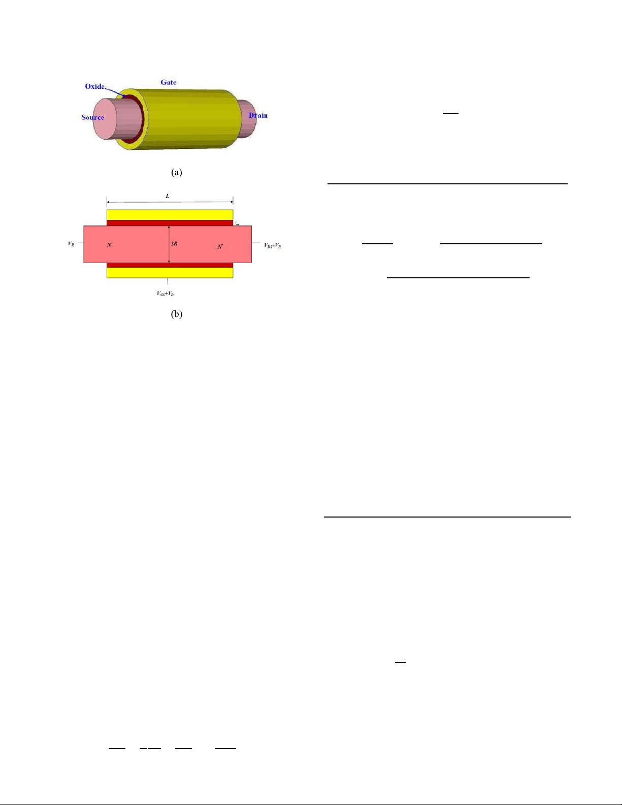
The schematic diagram of the device is shown in Fig. 1. The
gate length, gate oxide thickness, and silicon body radius of
a JLSG MOSFET are denoted by L, t
ox
,andR, respectively.
The Fermi level at the source end is chosen to be the reference
potential, V
R
.
A. Electric Potential
With the consideration of the symmetry, the PE in a
cylindrical coordinate can be expressed as
∂
2
φ
∂ρ
2
+
1
ρ
∂φ
∂ρ
+
∂
2
φ
∂z
2
=−
qN
D
ε
si
1 − exp
φ − V
V
t
(1)
0018-9383 © 2014 IEEE. Personal use is permitted, but republication/redistribution requires IEEE permission.
See http://www.ieee.org/publications_standards/publications/rights/index.html for more information.


 我的内容管理
展开
 我的资源
快来上传第一个资源
 我的收益 登录查看自己的收益
 我的积分
登录查看自己的积分
 我的C币
登录后查看C币余额
 我的收藏
我的收藏  我的下载
我的下载  下载帮助
下载帮助 
 前往需求广场,查看用户热搜

 信息提交成功