没有合适的资源?快使用搜索试试~ 我知道了~
V-F和F-V转换芯片_AD7740YRMZ-REEL7_规格书_ADI(亚德诺).PDF
需积分: 5 1 下载量 16 浏览量
2023-11-26
15:13:19
上传
评论
收藏 664KB PDF 举报
温馨提示
试读
12页
V-F和F-V转换芯片_AD7740YRMZ-REEL7_规格书_ADI(亚德诺)_LINEAR(凌特)模数转换芯片ADC规格书,中文数据手册,适合硬件电路设计开发人员使用。
资源推荐
资源详情
资源评论
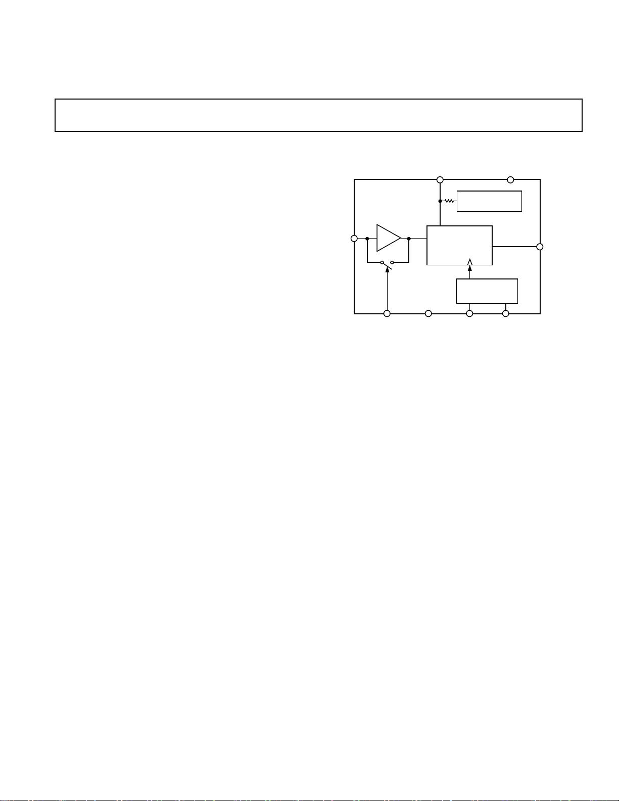
FUNCTIONAL BLOCK DIAGRAM
BUF
VDD
CLKIN
AD7740
VIN
FOUT
2.5V
REFERENCE
VOLTAGE-TO-
FREQUENCY
MODULATOR
CLKOUT
GND
CLOCK
GENERATION
REFIN/OUT
X1
a
AD7740*
FEATURES
Synchronous Operation
Full-Scale Frequency Set by External System Clock
8-Lead SOT-23 and 8-Lead MSOP Packages
3 V or 5 V Operation
Low Power: 3 mW (Typ)
Nominal Input Range: 0 to V
REF
True –150 mV Capability Without Charge Pump
V
REF
Range: 2.5 V to VDD
Internal 2.5 V Reference
1 MHz Max Input Frequency
Selectable High Impedance Buffered Input
Minimal External Components Required
APPLICATIONS
Isolation of High Common-Mode Voltages
Low-Cost Analog-to-Digital Conversion
Battery Monitoring
Automotive Sensing
GENERAL DESCRIPTION
The AD7740 is a low-cost, ultrasmall synchronous Voltage-to-
Frequency Converter (VFC). It works from a single 3.0 V to
3.6 V or 4.75 V to 5.25 V supply consuming 0.9 mA. The AD7740
is available in an 8-lead SOT-23 and also in an 8-lead MSOP
package. Small package, low cost and ease of use were major
design goals for this product. The part contains an on-chip 2.5 V
bandgap reference but the user may overdrive this using an
external reference. This external reference range includes VDD.
The full-scale output frequency is synchronous with the clock
signal on the CLKIN pin. This clock can be generated with the
addition of an external crystal (or resonator) or supplied from a
CMOS-compatible clock source. The part has a maximum
input frequency of 1 MHz.
For an analog input signal that goes from 0 V to V
REF
, the out-
put frequency goes from 10% to 90% of f
CLKIN.
In buffered mode,
the part provides a very high input impedance and accepts a
range of 0.1 V to VDD – 0.2 V on the VIN pin. There is also
an unbuffered mode of operation that allows VIN to go from
–0.15 V to VDD + 0.15 V. The modes are interchangeable using
the BUF pin.
The AD7740 (Y Grade) is guaranteed over the automotive
temperature range of –40°C to +105°C. The AD7740 (K Grade)
is guaranteed from 0°C to 85°C.
PRODUCT HIGHLIGHTS
1. The AD7740 is a single channel, single-ended VFC. It is
available in 8-lead SOT-23 and 8-lead MSOP packages, and is
intended for low-cost applications. The AD7740 offers
considerable space saving over alternative solutions.
2. The AD7740 operates from a single 3.0 V to 3.6 V or 4.75 V
to 5.25 V supply and consumes typically 0.9 mA when the
input is unbuffered. It also contains an automatic power-down
function.
3. The AD7740 does not require external resistors and capaci-
tors to set the output frequency. The maximum output
frequency is set by a crystal or a clock. No trimming or cali-
bration is required.
4. The analog input can be taken to 150 mV below GND for
true bipolar operation.
5. The specified voltage reference range on REFIN is from
2.5 V to the supply voltage, VDD.
3 V/5 V Low Power, Synchronous
Voltage-to-Frequency Converter
*Protected under U.S. Patent # 6,147,528.
Rev. C Document Feedback
Information furnished by Analog Devices is believed to be accurate and reliable. However, no
responsibility is assumed by Analog Devices for its use, nor for any infringements of patents or other
rights of third parties that may result from its use. Specifications subject to change without notice. No
license is granted by implication or otherwise under any patent or patent rights of Analog Devices.
Trademarks and registered trademarks are the property of their respective owners.
One Technology Way, P.O. Box 9106, Norwood, MA 02062-9106, U.S.A.
Tel: 781.329.4700 ©2001–2016 Analog Devices, Inc. All rights reserved.
Technical Support www.analog.com
功能框图
电压-频率调制
器
同步操作
由外部系统时钟8引线SOT-23和8引线MSOP封装设置的满
量程频率3 V或5 V工作低功率:3 mW (typp)标称输入范围:
0至V
REF
真-150 mV无充电泵能力 V
REF
范围:2.5 V至VDD内
部2.5 V参考1 MHz最大输入频率可选高阻抗缓冲输入所需
的最小外部元件
高共模电压隔离低成本模数转换电池监测汽车传
感
一般的描述
AD7740是一款低成本、超小型同步电压-频率转换器(VFC)。它的工
作从单个3.0 V到3.6 V或4.75 V到5.25 V的电源消耗0.9 mA。AD7740
有8引脚SOT-23和8引脚MSOP两种封装。小封装、低成本和易用性
是该产品的主要设计目标。该部分包含一个片上2.5 V带隙参考,但
用户可以使用外部参考过载。这个外部参考范围包括VDD。
满量程输出频率与CLKIN引脚上的时钟信号同步。该时钟可以通过
添加外部晶体(或谐振器)或由cmos兼容时钟源提供来生成。该部件
的最大输入频率为1mhz。
对于从0 V到 V
REF
的模拟输入信号,输出频率从 f
CLKIN.
的10%到90%。
在缓冲模式下,该部分提供了一个非常高的输入阻抗,并在VIN引
脚上接受0.1 V到VDD - 0.2 V的范围。还有一个无缓冲的操作模式
,允许VIN从-0.15 V到VDD + 0.15 V。使用BUF引脚可以互换模式
。
AD7740 (Y级)可保证在-40°C至+105°C的汽车温度范围内工作。AD
7740 (K级)的工作温度保证在0°C到85°C之间。
产品亮点
1. AD7740是一个单通道、单端VFC。它有8引脚SOT-23和8引脚MSO
P封装,适用于低成本应用。
的AD7740
与其他解决方案相比,节省了大量的空间。
2. AD7740的工作电压为3.0 V至3.6 V或4.75 V至5.25 V,输入无缓冲
时,功耗通常为0.9 mA。它还包含一个自动关机功能。
3.AD7740不需要外部电阻和电容来设置输出频率。最大输出频率
由晶体或时钟设定。不需要修边或校准。
4. 模拟输入可被置于地下150mv,以实现真正的双极操作。
5. REFIN上指定的参考电压范围是从2.5 V到电源电压VDD。
3v / 5v低功率,同步电压-
频率转换器
*受美国专利# 6,147,528保护。
文档反馈
我们相信adi公司提供的信息是准确可靠的。但是,Analog Devices对其使用不承担任何责
任,也不对因其使用而可能导致的任何侵犯第三方专利或其他权利的行为承担任何责任。
规格如有更改,恕不另行通知。adi公司的任何专利或专利权均未隐含或以其他方式授予许
可。商标和注册商标是其各自所有者的财产。
One Technology Way,邮编:02062-9106,诺伍德,美国,电话:781.329.47
00
©2001-2016 Analog Devices, Inc。版权所有。
技术支持
翻译仅供参考,如需更准确的信息,请参考英文版
AD7740 SPECIFICATIONS
K, Y Versions
1
Parameter
2
Min Typ Max Unit Test Conditions/Comments
DC PERFORMANCE
Integral Nonlinearity
CLKIN = 32 kHz
3
± 0.012 % of Span
4
Unbuffered Mode, External Clock at CLKIN
CLKIN = 1 MHz ± 0.012 % of Span Unbuffered Mode, Crystal at CLKIN
CLKIN = 32 kHz
3
± 0.018 % of Span Buffered Mode, External Clock at CLKIN
CLKIN = 1 MHz ± 0.018 % of Span Buffered Mode, Crystal at CLKIN
Offset Error ± 7 ± 35 mV Unbuffered Mode, VIN = 0 V
± 7 ± 35 mV Buffered Mode, VIN = 0.1 V
Gain Error ± 0.1 ± 0.7 % of Span
Offset Error Drift
3
± 20 µV/°C
Gain Error Drift
3
± 4 ppm of Span/°C
Power Supply Rejection Ratio
3
–55 dB ∆VDD = ± 5% (5 V)
–65 dB ∆VDD = ± 10% (3.3 V)
ANALOG INPUT, VIN
Nominal Input Span 0 – V
REF
V ± 150 mV Overrange Available
0.1 VDD – 0.2 V Buffered Mode
Input Current 8 10 µA Unbuffered Mode, VIN = 5.4 V, REFIN = 5.25 V
5 100 nA Buffered Mode, VIN = 0.1 V, REFIN = 2.5 V
REFERENCE VOLTAGE
REFIN
5
Nominal Input Voltage 2.5 VDD V
REFOUT
Output Voltage 2.3 2.5 2.7 V
Output Impedance
3
1kΩ See Pin Function Description
Reference Drift
3
± 50 ppm/°C
Line Rejection
3
–75 dB ∆VDD = ± 5% (5 V)
Line Rejection
3
–60 dB ∆VDD = ± 10% (3.3 V)
Reference Noise (0.1 Hz to 10 Hz)
3
100 µV p–p
FOUT OUTPUT
Nominal Frequency Span 0.1 f
CLKIN
to 0.9 f
CLKIN
Hz VIN = 0 V to V
REF
. See Figure 2
LOGIC INPUTS (CLKIN, BUF)
3
CLKIN
Input Frequency 32 1000 kHz For Specified Performance
Input High Voltage, V
IH
3.5 V VDD = 5 V ± 5%
Input High Voltage, V
IH
2.5 V VDD = 3.3 V ± 10%
Input Low Voltage, V
IL
0.8 V VDD = 5 V ± 5%
Input Low Voltage, V
IL
0.4 V VDD = 3.3 V ± 10%
Input Current ± 2 µA VIN = 0 V to V
DD
Pin Capacitance 3 10 pF
BUF
Input High Voltage, V
IH
2.4 V VDD = 5 V ± 5%
Input High Voltage, V
IH
2.1 V VDD = 3.3 V ± 10%
Input Low Voltage, V
IL
0.8 V VDD = 5 V ± 5%
Input Low Voltage, V
IL
0.4 V VDD = 3.3 V ± 10%
Input Current ± 100 nA
Pin Capacitance 3 10 pF
LOGIC OUTPUTS (FOUT, CLKOUT)
3
Output High Voltage, V
OH
4.0 V Output Sourcing 200 µA
6
. VDD = 5 V ± 5%
Output High Voltage, V
OH
2.1 V Output Sourcing 200 µA
6
. VDD = 3.3 V ± 10%
Output Low Voltage, V
OL
0.1 0.4 V Output Sinking 1.6 mA
6
POWER REQUIREMENTS
V
DD
7
3.0 5.25 V
I
DD
(Normal Mode)
8
0.9 1.25 mA V
IH
= VDD, V
IL
= GND. Unbuffered Mode
I
DD
(Normal Mode)
8
1.1 1.5 mA V
IH
= VDD, V
IL
= GND. Buffered Mode
I
DD
(Power-Down) 30 100 µA
Power-Up Time
3
30 µs Exiting Power-Down (Ext. Clock at CLKIN)
NOTES
1
Temperature range: K Version, 0°C to +85°C; Y Version, –40°C to +105°C; typical specifications are at 25°C.
2
See Terminology.
3
Guaranteed by design and characterization, not production tested.
4
Span = Max output frequency–Min output frequency.
5
Because this pin is bidirectional, any external reference must be capable of sinking/sourcing 400 µA in order to overdrive the internal reference.
6
These logic levels apply to CLKOUT only when it is loaded with one CMOS load.
7
Operation at VDD = 2.7 V is also possible with degraded specifications.
8
Outputs unloaded. I
DD
increases by C
L
× V
OUT
× f
FOUT
when FOUT is loaded. If using a crystal/resonator as the clock source, I
DD
will vary depending on the crystal/resonator
type (see Clock Generation section).
Specifications subject to change without notice.
REV. C
–2–
(VDD = 3.0 V to 3.6 V, 4.75 V to 5.25 V, GND = 0 V, REFIN = 2.5 V; CLKIN = 1 MHz; All
specifications T
MIN
to T
MAX
unless otherwise noted.)
AD7740规范
测试条件/评论
直流性能积分非线性CLKI
N = 32 kHz
3
无缓冲模式,外部时钟在CLKIN
CLKIN = 1 MHz 无缓冲模式,水晶在CLKIN
缓冲模式,外部时钟在CLKIN
CLKIN = 1 MHz 缓冲模式,水晶在CLKIN
偏置误差 无缓冲模式,VIN = 0 V
缓冲模式,VIN = 0.1 V
增益误差
偏移错误 Drift
3
增益错误 Drift
3
ppm跨度/°C
电源拒接 Ratio
3
VDD =±5% (5 v)
VDD =±10% (3.3 v)
模拟输入,VIN标称输入
量程
±150mv超量程可用
缓冲模式
输入电流 无缓冲模式,VIN = 5.4 V, REFIN = 5.25 V
缓冲模式,VIN = 0.1 V, REFIN = 2.5 V
参考电压
标称输入电压
REFOUT输出电压
参见引脚功能说明
VDD =±5% (5 v)
VDD =±10% (3.3 v)
参考噪声(0.1 Hz至10 Hz)
3
4输出标称频率范围
0.1f
CLKIN
至0.9f
CLKIN
VIN = 0 V至 V
REF
。参见图2
逻辑输入(CLKIN, BUF)
3
CLKIN输入频
率
指定性能
输入高压, V
IH
VDD = 5v±5%
输入高压, V
IH
VDD = 3.3 v±10%
输入低电压, V
IL
VDD = 5v±5%
输入低电压, V
IL
VDD = 3.3 v±10%
输入电流
VIN = 0 V至 V
DD
销电容
输入高压, V
IH
VDD = 5v±5%
输入高压, V
IH
VDD = 3.3 v±10%
输入低电压, V
IL
VDD = 5v±5%
输入低电压, V
IL
VDD = 3.3 v±10%
输入电流
销电容
逻辑输出(FOUT, CLKOUT)
3
输出高压, V
OH
输出源200µ A
6
.VDD = 5 V±5%
输出高压, V
OH
输出源200µ A
6
. VDD = 3.3 V ±10%
输出低电压, V
OL
输出下沉1.6 mA
6
功率要求
V
IH
= vdd, V
IL
= gnd。无缓冲的模式
V
IH
= vdd, V
IL
= gnd。缓冲模式
正在退出电源关闭(例如时钟在CLKIN)
温度范围:K版,0°C至+85°C;Y型,-40°C至+105°C;典型规格为25°C。
看到术语。
由设计和特性保证,而不是生产测试。
Span =最大输出频率-最小输出频率。
由于该引脚是双向的,因此任何外部基准都必须能够下沉/输入400µA,以超速驱动内部基准。
这些逻辑电平仅在CLKOUT加载一个CMOS负载时才适用于它。
操作在VDD = 2.7 V也可能与降级规格。
输出卸载。当FOUT加载时, I
DD
增加C
L
×V
OUT
×f
FOUT
如果使用晶体/谐振器作为时钟源, I
DD
将根据晶体/谐振器类型而变化(参见时钟生成部分)。规格如有更改,恕不另行通知。
(VDD = 3.0 V ~ 3.6 V, 4.75 V ~ 5.25 V, GND = 0 V, REFIN = 2.5 V;CLKIN
= 1 MHz;所有规格 T
MIN
至T
MAX
,除非另有说明。)
AD7740
REV. C
–3–
(VDD = 3.0 V to 3.6 V, 4.75 V to 5.25 V, GND = O V, REFIN = 2.5 V)
Limit at T
MIN
, T
MAX
Limit at T
MIN
, T
MAX
Parameter VDD = 3.0 V to 3.6 V VDD = 4.75 V to 5.25 V Unit Conditions/Comments
f
CLKIN
32 32 kHz min Clock Frequency
1 1 MHz max
t
HIGH
:t
LOW
40:60 40:60 min Clock Mark/Space Ratio
60:40 60:40 max
t
1
50 35 ns typ CLKIN Edge to FOUT Edge Delay
t
2
2.3 1.8 ns typ FOUT Rise Time
t
3
1.6 1.4 ns typ FOUT Fall Time
t
4
t
HIGH
± 20
t
HIGH
± 8
ns typ FOUT Pulsewidth
NOTES
1
Guaranteed by design and characterization, not production tested.
2
All input signals are specified with tr = tf = 5 ns (10% to 90% of VDD) and timed from a voltage level of (V
IL
+ V
IH
)/2.
3
See Figure 1.
Specifications subject to change without notice.
t
3
t
2
t
1
t
4
t
HIGH
t
LOW
CLKIN
FOUT
Figure 1. Timing Diagram
TIMING CHARACTERISTICS
1, 2, 3
ABSOLUTE MAXIMUM RATINGS*
(T
A
= 25°C unless otherwise noted)
VDD to GND . . . . . . . . . . . . . . . . . . . . . . . . . –0.3 V to +7 V
Analog Input Voltage to GND . . . . . . . . –0.3 V to V
DD
+ 0.3 V
Reference Input Voltage to GND . . . . . –0.3 V to V
DD
+ 0.3 V
Logic Input Voltage to GND . . . . . . . . –0.3 V to VDD + 0.3 V
FOUT Voltage to GND . . . . . . . . . . . –0.3 V to VDD + 0.3 V
Operating Temperature Range
Commercial (K Version) . . . . . . . . . . . . . . . . 0°C to +85°C
Automotive (Y Version) . . . . . . . . . . . . . . –40°C to +105°C
Storage Temperature Range . . . . . . . . . . . . –65°C to +150°C
Junction Temperature (T
J
Max) . . . . . . . . . . . . . . . . . . 150°C
SOT-23 Package
Power Dissipation . . . . . . . . . . . . . . . . . . (T
J
Max – T
A
)/θ
JA
θ
JA
Thermal Impedance . . . . . . . . . . . . . . . . . . . . . 240°C/W
Lead Temperature (10 secs) . . . . . . . . . . . . . . . . . . 300°C
Reflow Soldering
Peak Temperature . . . . . . . . . . . . . . . . . . . . 220 + 5/0°C
Time at Peak Temperature . . . . . . . . . . . . 10 sec to 40 sec
MSOP Package
Power Dissipation . . . . . . . . . . . . . . . . . (T
J
Max – T
A
)/θ
JA
θ
JA
Thermal Impedance . . . . . . . . . . . . . . . . . . . . . 206°C/W
θ
JC
Thermal Impedance . . . . . . . . . . . . . . . . . . . . . . 44°C/W
Lead Temperature (10 secs) . . . . . . . . . . . . . . . . . . . 300°C
Reflow Soldering
Peak Temperature . . . . . . . . . . . . . . . . . . . . . . 220 +5/0°C
Time at Peak Temperature . . . . . . . . . . . . . 10 sec to 40 sec
*Stresses above those listed under Absolute Maximum Ratings may cause perma-
nent damage to the device. This is a stress rating only; functional operation of the
device at these or any other conditions above those listed in the operational
sections of this specification is not implied. Exposure to absolute maximum rating
conditions for extended periods may affect device reliability.
CAUTION
ESD (electrostatic discharge) sensitive device. Electrostatic charges as high as 4000 V readily
accumulate on the human body and test equipment and can discharge without detection. Although
the AD7740 features proprietary ESD protection circuitry, permanent damage may occur on
devices subjected to high-energy electrostatic discharges. Therefore, proper ESD precautions are
recommended to avoid performance degradation or loss of functionality.
WARNING!
ESD SENSITIVE DEVICE
(VDD = 3.0 V ~ 3.6 V, 4.75 V ~ 5.25 V, GND = 0 V, REFIN = 2.5 V)
极限在 T
MIN
、T
MAX
限制在 T
MIN
、T
MAX
VDD = 3.0 V ~ 3.6 V VDD = 4.75 V至5.25 V
赫兹的最小值 时钟频率
MHz马克斯
时钟标记/空间比率
ns typ 点击边缘到FOUT边缘延迟
ns typ 四、上升时间
ns typ 四、下降时间
ns typ 输出信号脉冲宽度
由设计和特性保证,而不是生产测试。
所有输入信号都指定为tr = tf = 5 ns (VDD的10%至90%),并从 (V
IL
+V
IH
电压电平计时。
参见图1。
规格如有更改,恕不另行通知。
图1所示。时间图
时间特征
绝对最大评级*
(T
A
= 25°C(除非另有说明)
VDD,接地 . . . . . . . . . . . . . . . . . . . . . . . . . -0.3V至+ 7v
模拟输入电压到地. . . . . . . .-0.3V至 V
DD
+ 0.3V基准输入电压至GND . .
. . .-0.3 V到 V
DD
+ 0.3 V逻辑输入电压到GND . . . . . . . .-0.3 V转VDD +
0.3 V FOUT转地电压. . . . . . . . . . .-0.3 V至VDD + 0.3 V工作温度范围
商用(K版). . . . . . . . . . . . . . . .0°C + 85°C汽车(Y版本 ) . . . . . . . . . . . . . .
-40℃~ +105℃
储存温度范围. . . . . . . . . . . . -65℃~ +150℃
结温(T
J
Max ) . . . . . . . . . . . . . . . . . .150°C SOT-23封装功耗. . . . . . . . . . .
. . . . . . . (T
J
Max - T
A
)/θ
JA
JA热阻抗 . . . . . . . . . . . . . . . . . . . . .240°c / w
导致温度(10秒 ) . . . . . . . . . . . . . . . . . .300°C
再流焊
峰值温度 . . . . . . . . . . . . . . . . . . . .
峰值温度时间. . . . . . . . . . . .10秒到40秒
MSOP包
功耗 . . . . . . . . . . . . . . . . .
JA热阻抗 . . . . . . . . . . . . . . . . . . . . .206°c / w
JC热阻抗 . . . . . . . . . . . . . . . . . . . . . .44°c / w
导致温度(10秒 ) . . . . . . . . . . . . . . . . . . .300°C回流焊峰值温度. . . . . .
. . . . . . . . . . . . . . . .220 +5/0°C峰值温度时间. . . . . . . . . . . . .10秒到4
0秒
*高于绝对最大额定值的应力可能会对设备造成永久性损坏。这只是一个压力等级;不暗
示设备在这些或上述本说明书操作部分所列的任何其他条件下的功能操作。长时间暴
露在绝对最大额定值条件下可能会影响设备的可靠性。
ESD(静电放电)敏感器件。高达4000v的静电电荷很容易在人体和测试设备上积累,并且可以在不被检测到
的情况下放电。虽然AD7740具有专有的ESD保护电路,但高能静电放电可能会对器件造成永久性损坏。因
此,建议采取适当的防静电措施,避免设备性能下降或功能丧失。
静电敏感器件
剩余11页未读,继续阅读
资源评论
沐风听雨_A
- 粉丝: 300
- 资源: 183
上传资源 快速赚钱
- 我的内容管理 展开
- 我的资源 快来上传第一个资源
- 我的收益 登录查看自己的收益
- 我的积分 登录查看自己的积分
- 我的C币 登录后查看C币余额
- 我的收藏
- 我的下载
- 下载帮助
安全验证
文档复制为VIP权益,开通VIP直接复制
信息提交成功