没有合适的资源?快使用搜索试试~ 我知道了~
SKY67102-396LF 射频放大器
需积分: 10 1 下载量 87 浏览量
2022-09-16
16:11:27
上传
评论
收藏 1.18MB PDF 举报
温馨提示
试读
12页
SKY67102-396LF 射频放大器
资源推荐
资源详情
资源评论
Skyworks Solutions, Inc. • Phone [781] 376-3000 • Fax [781] 376-3100 • sales@skyworksinc.com • www.skyworksinc.com
201631B • Skyworks Proprietary Information • Products and Product Information are Subject to Change Without Notice • September 28, 2011 1
DATA SHEET
SKY67102-396LF: 2.0-3.0 GHz High Linearity, Active Bias
Low-Noise Amplifier
Applications
• CDMA, WCDMA, TD-SCDMA, WiMAX, and LTE cellular
infrastructure
• Ultra low-noise systems
Features
• Ultra Low Noise Figure: 0.8 dB @ 2.6 GHz
• Input and output return loss > 18 dB @ 2.6 GHz
• High IIP3 performance: +16.7 dBm @ 2.6 GHz
• Adjustable supply current and gain
• Temperature and process-stable active bias
• Miniature DFN (8-pin, 2 x 2 mm) package (MSL1 @ 260 °C per
JEDEC J-STD-020)
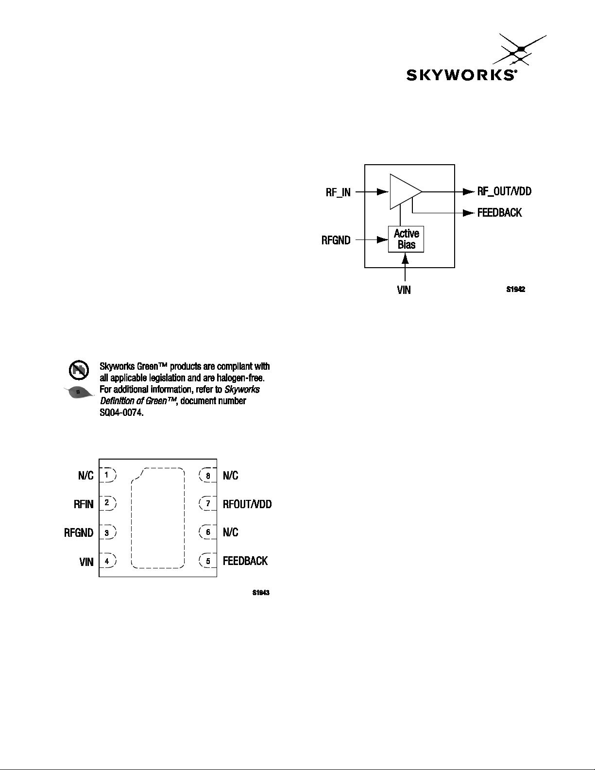
Figure 2. SKY67102-396LF Pinout – 8-Pin DFN
(Top View)
Figure 1. SKY67102-396LF Block Diagram
Description
The SKY67102-396LF is GaAs, pHEMT Low-Noise Amplifier (LNA)
with an active bias and high linearity performance. The advanced
GaAs pHEMT enhancement mode process provides excellent
return loss, low noise, and high linearity performance.
The internal active bias circuitry provides stable performance over
temperature and process variation. The device offers the ability to
externally adjust supply current and gain. Supply voltage is
applied to the RFOUT/VDD pin through an RF choke inductor. Pin 4
(VIN) should be connected to RFOUT/VDD through an external
resistor to control the supply current. The RFIN and RFOUT/VDD
pins should be DC blocked to ensure proper operation. Pin 5
(FEEDBACK) is connected through an RC network to externally
adjust the gain of the device without affecting the Noise Figure
(NF) of the LNA.
The SKY67102-396LF operates in the frequency range of 2.0 to
3.0 GHz with proper tuning. For lower frequency operation, the
pin-compatible SKY67100-396LF or SKY67101-396LF should be
used.
The LNA is manufactured in a compact, 2 x 2 mm, 8-pin Dual Flat
No-Lead (DFN) package. A functional block diagram is shown in
Figure 1. The pin configuration and package are shown in
Figure 2. Signal pin assignments and functional pin descriptions
are provided in Table 1.
DATA SHEET • SKY67102-396LF HIGH LINEARITY, ACTIVE BIAS LNA
Skyworks Solutions, Inc. • Phone [781] 376-3000 • Fax [781] 376-3100 • sales@skyworksinc.com • www.skyworksinc.com
2 September 28, 2011 • Skyworks Proprietary Information • Products and Product Information are Subject to Change Without Notice • 201631B
Table 1. SKY67102-396LF Signal Descriptions
Pin # Name Description Pin # Name Description
1 N/C No connection. May be connected to ground
with no change in performance.
5 FEEDBACK LNA external gain control. Connect to
RFOUT using a series RD network.
2 RFIN RF input. DC blocking capacitor required. 6 N/C No connection. May be connected to ground
with no change in performance.
3 RFGND RF ground. Connect to ground through a
capacitor.
7 RFOUT/VDD RF output. Apply VDD through RF choke
inductor. DC blocking capacitor required.
4 VIN LNA supply current. Connect through series
resistor to VDD.
8 N/C No connection. May be connected to ground
with no change in performance.
Table 2. SKY67102-396LF Absolute Maximum Ratings
Parameter Symbol Minimum Typical Maximum Units
Supply voltage VDD 5.5 V
Supply current IDD 100 mA
RF input power PIN +20 dBm
Storage temperature TSTG –65 +25 +125 °C
Operating temperature TA –40 +25 +85 °C
Junction temperature TJ +150 °C
Notes: Exposure to maximum rating conditions for extended periods may reduce device reliability. There is no damage to device with only one parameter set at the limit and all other
parameters set at or below their nominal value. Exceeding any of the limits listed here may result in permanent damage to the device.
Thermal resistance = 83 °C/W @ 4 V bias.
CAUTION: Although this device is designed to be as robust as possible, Electrostatic Discharge (ESD) can damage this device. This device
must be protected at all times from ESD. Static charges may easily produce potentials of several kilovolts on the human body
or equipment, which can discharge without detection. Industry-standard ESD precautions should be used at all times. The
SKY67102-396LF is a Human Body Model (HBM) Class 1A ESD device.
Electrical and Mechanical Specifications
The absolute maximum ratings of the SKY67102-396LF are
provided in Table 2. Electrical specifications are provided in
Table 3.
Typical performance characteristics of the SKY67102-396LF are
illustrated in Figures 3 through 14.
DATA SHEET • SKY67102-396LF HIGH LINEARITY, ACTIVE BIAS LNA
Skyworks Solutions, Inc. • Phone [781] 376-3000 • Fax [781] 376-3100 • sales@skyworksinc.com • www.skyworksinc.com
201631B • Skyworks Proprietary Information • Products and Product Information are Subject to Change Without Notice • September 28, 2011 3
Table 3. SKY67102-396LF Electrical Specifications (Note 1)
(V
DD = 4.0 V, IDD = 50 mA, TA = +25 °C, PIN = –20 dBm, Characteristic Impedance [ZO] = 50 Ω, Unless Otherwise Noted)
Parameter Symbol Test Condition Min Typical Max Units
RF Specifications
Noise Figure (Note 2) NF @ 2.0 GHz
@ 2.6 GHz
@ 3.0 GHz
1.10
0.80
1.10
0.95
dB
dB
dB
Small signal gain |S21| @ 2.0 GHz
@ 2.6 GHz
@ 3.0 GHz
16.2
18.2
17.2
1.12
18.2
dB
dB
dB
Input return loss |S11| @ 2.0 GHz
@ 2.6 GHz
@ 3.0 GHz
15
10
18
12
dB
dB
dB
Output return loss |S22| @ 2.0 GHz
@ 2.6 GHz
@ 3.0 GHz
14
9
17
13
dB
dB
dB
Reverse isolation |S12| @ 2.0 GHz
@ 2.6 GHz
@ 3.0 GHz
34
37
37
38
dB
dB
dB
3
rd
Order Input Intercept Point IIP3 @ 2.6 GHz, Δf = 5 MHz,
P
IN = –18 dBm/tone
+16.7 dBm
3
rd
Order Output Intercept Point OIP3 @ 2.6 GHz, Δf = 5 MHz,
P
IN = –18 dBm/tone
+32.0 +33.8 dBm
1 dB Input Compression Point IP1dB @ 2.6 GHz –1 dBm
1 dB Output Compression Point OP1dB @ 2.6 GHz +15.1 dBm
Stability μ1, μ2 Up to 18 GHz,
–40 °C to +85 °C
>1 –
DC Specifications
Supply voltage VDD 3.3 4.0 5.0 V
Supply current IDD Set with external resistor 15 50 90 mA
Note 1: Performance is guaranteed only under the conditions listed in this Table.
Note 2 Loss from the input SMA connector and Evaluation Board up to component C1 has been de-embedded from the NF measurement.
剩余11页未读,继续阅读
资源评论
shijuntao1985
- 粉丝: 1
- 资源: 72
上传资源 快速赚钱
- 我的内容管理 展开
- 我的资源 快来上传第一个资源
- 我的收益 登录查看自己的收益
- 我的积分 登录查看自己的积分
- 我的C币 登录后查看C币余额
- 我的收藏
- 我的下载
- 下载帮助
最新资源
- 51单片机学习(1)-软件keil下载
- 历届(第1-21届)希望杯数学竞赛初一试题及答案(最新整理).doc全国数学邀请赛(264页资料)
- 水滴.psd
- TokenPocket_V2.1.2_release.apk
- Apache-druid-kafka-rce.yaml
- 基于C#的ASP.NET数据库原理及应用技术课程指导平台的开发
- 基于ROS的智能车轨迹跟踪算法的仿真与设计源码运用PID跟踪算法.zip.zip
- Bug Bounty Tip - i春秋Self-XSS变废为宝的奇思妙想
- 1991-2015年全国初中化学竞赛复赛试题汇编(212页)(24年竞赛复赛真题).docx天原杯
- Apache Flink 未授权访问+远程代码执行.pdf
资源上传下载、课程学习等过程中有任何疑问或建议,欢迎提出宝贵意见哦~我们会及时处理!
点击此处反馈
安全验证
文档复制为VIP权益,开通VIP直接复制
信息提交成功