design_of_switch_phaseshifter_MMICs
需积分: 5 195 浏览量
2022-09-14
11:43:02
上传
评论
收藏 394KB PDF 举报

∗
∗∗
∗
Liam Devlin is with Plextek Communications Technology Consultants, London Road, Great Chesterford, Essex,
CB10 1NY Tel: +44 (0)1799 533200 Fax: +44 (0)1799 533201 Email: lmd@plextek.co.uk
The Design of Integrated Switches and Phase Shifters
Liam Devlin
∗
∗∗
∗
Abstract
Integrated analogue switches can easily be designed using any Field Effect Transistor (FET) based process
[1]. The challenges in switch design tend to come in extending the upper operating frequency and/or
increasing the power handling capability. The first part of this paper describes the operation of FETs as
switches and presents design techniques for realising integrated RF and microwave switches. Consideration is
also given to techniques for improving the power handling capability of switch designs.
Phase shifting circuits allow control of the
insertion phase of a network. They find
applications in electronic beam-forming,
channel matching networks and measurement
systems. The second part of this paper details
phase shifting techniques suitable for
integrated realisations. Analogue and digitally
controlled techniques are included and
examples of phase shifter designs are
presented.
Switch Design - Introduction
The FET’s suitability for switch realisation stems
from the fact that its drain-source resistance
behaves as a voltage variable resistor, the resistance
being set by the gate-source voltage. When used as
a switch, a FET is operated with the drain and
source at zero volts DC. The RF signal path is drain
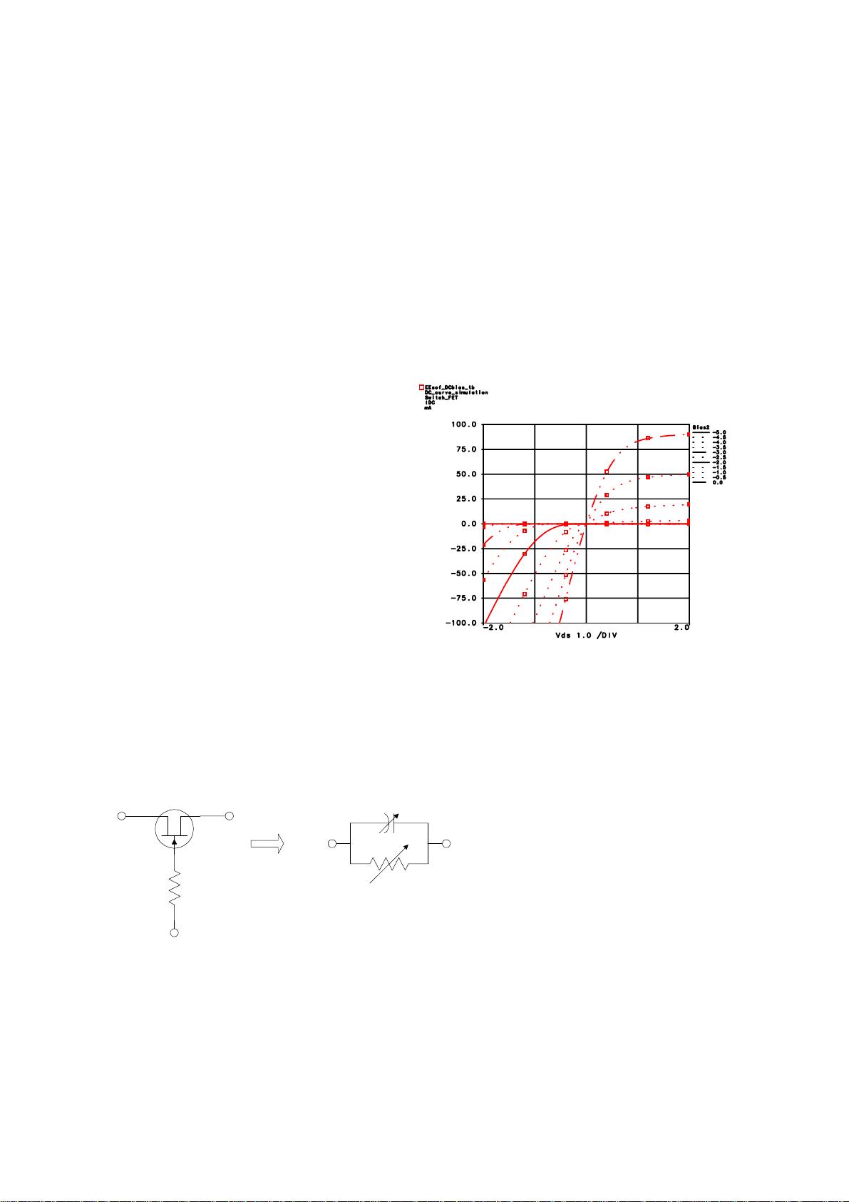
to source and the gate is the control terminal. Figure 1 shows the typical I-V characteristics of a depletion mode FET
about the Vds=0V point, for different (negative) Vgs bias voltages.
It can be seen that, in the region of
Vds=0V, the Vds/Ids characteristic
approximates a resistance (Ids ∝ Vds). For
Vgs=0V this is a low resistance (the FET is
on) and for Vgs below pinch-off, the FET is
off and presents a high resistance. This
gives rise to the simple approximate
equivalent circuit, shown in Figure 2. The
gate resistor (Rg) is included as a simple
and effective means of providing extra
isolation between the signal and control
path, a value of several kΩ is typically
used. It is possible to use such a simple biasing technique because FETs draw very little gate current
(typically < 0.5mA/mm for high gate-drain voltages and decreasing for lower). The very low DC power
consumption of FET based switches is a significant advantage compared to PIN diode based switch designs.
Figure 1: DC characteristics of a FET in the region o
f
switch operation
Rg
Vg
Fi
g
ure 2: A
pp
roximate e
q
uivalent circuit of a switchin
g

剩余14页未读,继续阅读


评论0
最新资源