没有合适的资源?快使用搜索试试~ 我知道了~
:LM629 是一款电机专用运动控制处理器,可用于直流、无刷直流电机及其它可提供增量式位置反馈信号的伺服机 构。该器件可完成数字运动控制中的高精度实时计算任务。根据LM629 功能特点与工作原理,以LM629 为核心构建了微型 位置伺服控制系统。介绍该系统的硬件结构,详细讨论了软件开发流程。LM629 的使用简化了系统结构,加快了运动控制模 块的开发进度。
资源详情
资源评论
资源推荐
LM628/LM629
Precision Motion Controller
General Description
The LM628/LM629 are dedicated motion-control processors
designed for use with a variety of DC and brushless DC
servo motors, and other servomechanisms which provide a
quadrature incremental position feedback signal. The parts
perform the intensive, real-time computational tasks required
for high performance digital motion control. The host control
software interface is facilitated by a high-level command set.
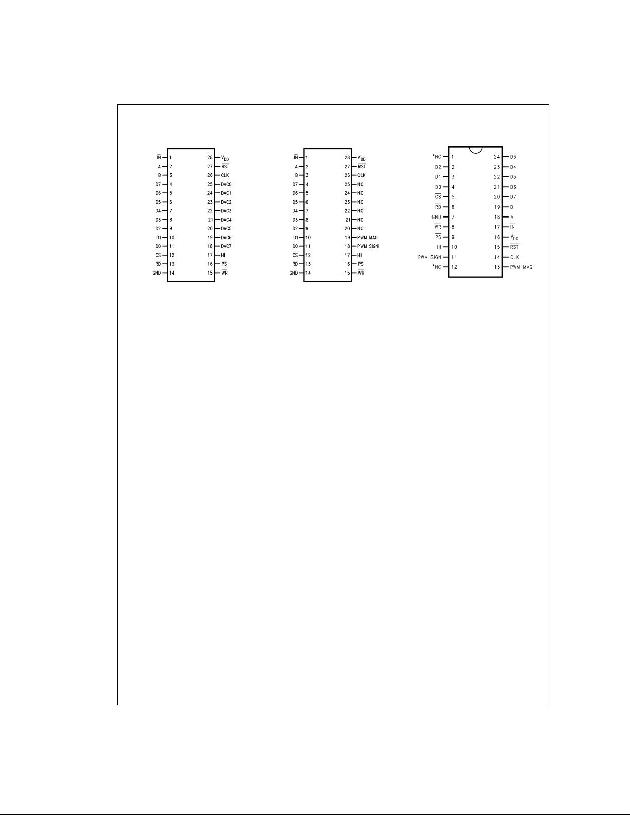
The LM628 has an 8-bit output which can drive either an
8-bit or a 12-bit DAC. The components required to build a
servo system are reduced to the DC motor/actuator, an in-
cremental encoder, a DAC, a power amplifier, and the
LM628. An LM629-based system is similar, except that it
provides an 8-bit PWM output for directly driving H-switches.
The parts are fabricated in NMOS and packaged in a 28-pin
dual in-line package or a 24-pin surface mount package
(LM629 only). Both 6 MHz and 8 MHz maximum frequency
versions are available with the suffixes -6 and -8, respec-
tively, used to designate the versions. They incorporate an
SDA core processor and cells designed by SDA.
Features
n 32-bit position, velocity, and acceleration registers
n Programmable digital PID filter with 16-bit coefficients
n Programmable derivative sampling interval
n 8- or 12-bit DAC output data (LM628)
n 8-bit sign-magnitude PWM output data (LM629)
n Internal trapezoidal velocity profile generator
n Velocity, target position, and filter parameters may be
changed during motion
n Position and velocity modes of operation
n Real-time programmable host interrupts
n 8-bit parallel asynchronous host interface
n Quadrature incremental encoder interface with index
pulse input
n Available in a 28-pin dual in-line package or a 24-pin
surface mount package (LM629 only)
TRI-STATE
®
is a registered trademark of National Semiconductor Corporation.
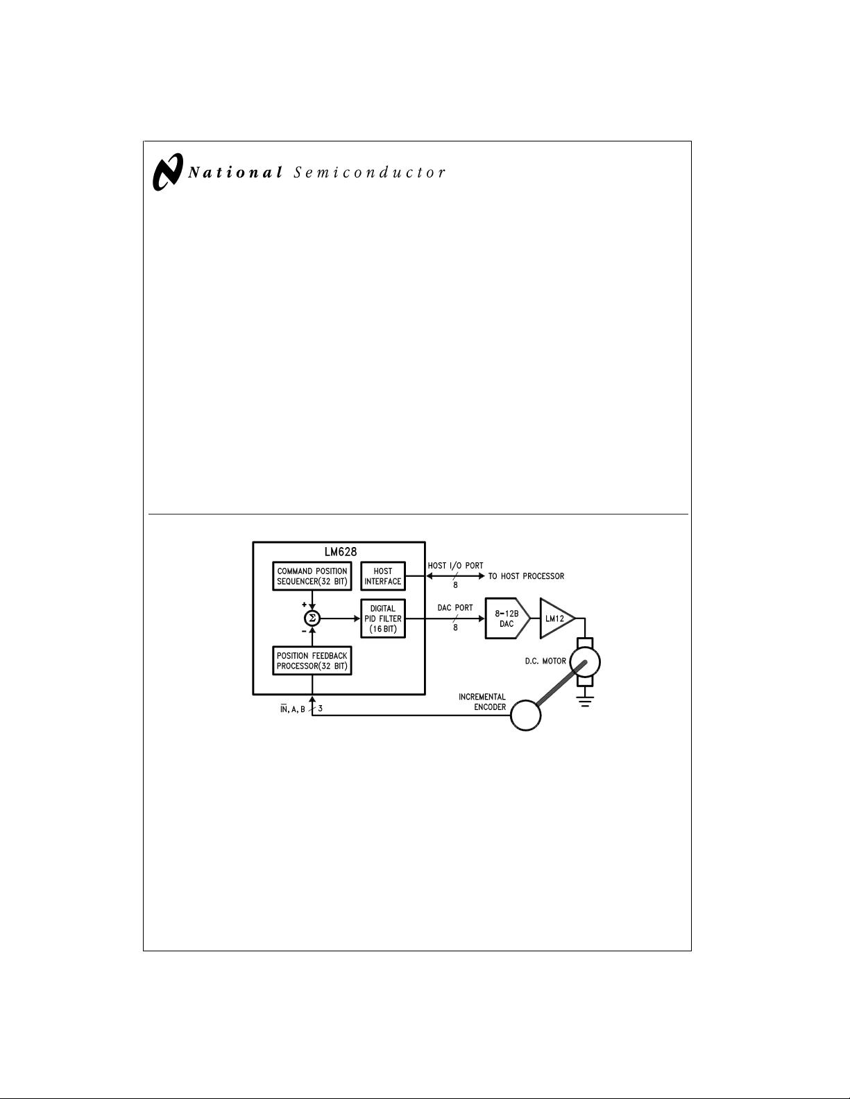
DS009219-1
FIGURE 1. Block Diagram
November 1999
LM628/LM629 Precision Motion Controller
© 1999 National Semiconductor Corporation DS009219 www.national.com
Connection Diagrams
LM628N
DS009219-2
LM629N
DS009219-3
LM629M
DS009219-21
*Do not connect.
Order Number LM629M-6, LM629M-8, LM628N-6, LM628N-8, LM629N-6 or LM629N-8
See NS Package Number M24B or N28B
LM628/LM629
www.national.com 2
Absolute Maximum Ratings (Note 1)
If Military/Aerospace specified devices are required,
please contact the National Semiconductor Sales Office/
Distributors for availability and specifications.
Voltage at Any Pin with
Respect to GND −0.3V to +7.0V
Ambient Storage Temperature −65˚C to +150˚C
Lead Temperature
28-pin Dual In-Line
Package (Soldering, 4 sec.) 260˚C
24-pin Surface Mount
Package (Soldering, 10 sec.) 300˚C
Maximum Power Dissipation
(T
A
≤ 85˚C, (Note 2) 605 mW
ESD Tolerance
(C
ZAP
=
120 pF, R
ZAP
=
1.5k) 2000V
Operating Ratings
Temperature Range −40˚C
<
T
A
<
+85˚C
Clock Frequency:
LM628N-6, LM629N-6,
LM629M-6 1.0 MHz
<
f
CLK
<
6.0 MHz
LM628N-8, LM629N-8,
LM629M-8 1.0 MHz
<
f
CLK
<
8.0 MHz
V
DD
Range 4.5V
<
V
DD
<
5.5V
DC Electrical Characteristics
(V
DD
and T
A
per Operating Ratings; f
CLK
=
6 MHz)
Symbol Parameter Conditions Tested Limits Units
Min Max
I
DD
Supply Current Outputs Open 110 mA
INPUT VOLTAGES
V
IH
Logic 1 Input Voltage 2.0 V
V
IL
Logic 0 Input Voltage 0.8 V
I
IN
Input Currents 0 ≤ V
IN
≤ V
DD
−10 10 µA
OUTPUT VOLTAGES
V
OH
Logic 1 I
OH
=
−1.6 mA 2.4 V
V
OL
Logic 0 I
OL
=
1.6 mA 0.4 V
I
OUT
TRI-STATE
®
Output Leakage Current 0 ≤ V
OUT
≤ V
DD
−10 10 µA
AC Electrical Characteristics
(V
DD
and T
A
per Operating Ratings; f
CLK
=
6 MHz; C
LOAD
=
50 pF; Input Test Signal t
r
=
t
f
=
10 ns)
Timing Interval T
#
Tested Limits Units
Min Max
ENCODER AND INDEX TIMING (See
Figure 2
)
Motor-Phase Pulse Width T1
µs
Dwell-Time per State T2
µs
Index Pulse Setup and Hold T3 0 µs
(Relative to A and B Low)
CLOCK AND RESET TIMING (See
Figure 3
)
Clock Pulse Width
LM628N-6, LM629N-6, LM629M-6 T4 78 ns
LM628N-8, LM629N-8, LM629M-8 T4 57 ns
Clock Period
LM628N-6, LM629N-6, LM629M-6 T5 166 ns
LM628N-8, LM629N-8, LM629M-8 T5 125 ns
Reset Pulse Width T6
µs
LM628/LM629
www.national.com3
AC Electrical Characteristics (Continued)
(V
DD
and T
A
per Operating Ratings; f
CLK
=
6 MHz; C
LOAD
=
50 pF; Input Test Signal t
r
=
t
f
=
10 ns)
Timing Interval T
#
Tested Limits Units
Min Max
STATUS BYTE READ TIMING (See
Figure 4
)
Chip-Select Setup/Hold Time T7 0 ns
Port-Select Setup Time T8 30 ns
Port-Select Hold Time T9 30 ns
Read Data Access Time T10 180 ns
Read Data Hold Time T11 0 ns
RD High to Hi-Z Time
T12 180 ns
COMMAND BYTE WRITE TIMING (See
Figure 5
)
Chip-Select Setup/Hold Time T7 0 ns
Port-Select Setup Time T8 30 ns
Port-Select Hold Time T9 30 ns
Busy Bit Delay T13 (Note 3) ns
WR Pulse Width
T14 100 ns
Write Data Setup Time T15 50 ns
Write Data Hold Time T16 120 ns
DATA WORD READ TIMING (See
Figure 6
)
Chip-Select Setup/Hold Time T7 0 ns
Port-Select Setup Time T8 30 ns
Port-Select Hold Time T9 30 ns
Read Data Access Time T10 180 ns
Read Data Hold Time T11 0 ns
RD High to Hi-Z Time
T12 180 ns
Busy Bit Delay T13 (Note 3) ns
Read Recovery Time T17 120 ns
DATA WORD WRITE TIMING (See
Figure 7
)
Chip-Select Setup/Hold Time T7 0 ns
Port-Select Setup Time T8 30 ns
Port-Select Hold Time T9 30 ns
Busy Bit Delay T13 (Note 3) ns
WR Pulse Width
T14 100 ns
Write Data Setup Time T15 50 ns
Write Data Hold Time T16 120 ns
Write Recovery Time T18 120 ns
Note 1: Absolute Maximum Ratings indicate limits beyond which damage to the device may occur. DC and AC electrical specifications do not apply when operating
the device beyond the above Operating Ratings.
Note 2: When operating at ambient temperatures above 70˚C, the device must be protected against excessive junction temperatures. Mounting the package on a
printed circuit board having an area greater than three square inches and surrounding the leads and body with wide copper traces and large, uninterrupted areas of
copper, such as a ground plane, suffices. The 28-pin DIP (N) and the 24-pin surface mount package (M) are molded plastic packages with solid copper lead frames.
Most of the heat generated at the die flows from the die, through the copper lead frame, and into copper traces on the printed circuit board. The copper traces act
as a heat sink. Double-sided or multi-layer boards provide heat transfer characteristics superior to those of single-sided boards.
Note 3: In order to read the busy bit, the status byte must first be read. The time required to read the busy bit far exceeds the time the chip requires to set the busy
bit. It is, therefore, impossible to test actual busy bit delay. The busy bit is guaranteed to be valid as soon as the user is able to read it.
LM628/LM629
www.national.com 4
AC Electrical Characteristics (Continued)
DS009219-4
FIGURE 2. Quadrature Encoder Input Timing
DS009219-5
FIGURE 3. Clock and Reset Timing
DS009219-6
FIGURE 4. Status Byte Read Timing
LM628/LM629
www.national.com5
剩余23页未读,继续阅读
sdm110110
- 粉丝: 0
- 资源: 2
上传资源 快速赚钱
- 我的内容管理 展开
- 我的资源 快来上传第一个资源
- 我的收益 登录查看自己的收益
- 我的积分 登录查看自己的积分
- 我的C币 登录后查看C币余额
- 我的收藏
- 我的下载
- 下载帮助
最新资源
- 51单片机学习(1)-软件keil下载
- 历届(第1-21届)希望杯数学竞赛初一试题及答案(最新整理).doc全国数学邀请赛(264页资料)
- 水滴.psd
- TokenPocket_V2.1.2_release.apk
- Apache-druid-kafka-rce.yaml
- 基于C#的ASP.NET数据库原理及应用技术课程指导平台的开发
- 基于ROS的智能车轨迹跟踪算法的仿真与设计源码运用PID跟踪算法.zip.zip
- Bug Bounty Tip - i春秋Self-XSS变废为宝的奇思妙想
- 1991-2015年全国初中化学竞赛复赛试题汇编(212页)(24年竞赛复赛真题).docx天原杯
- Apache Flink 未授权访问+远程代码执行.pdf
资源上传下载、课程学习等过程中有任何疑问或建议,欢迎提出宝贵意见哦~我们会及时处理!
点击此处反馈
安全验证
文档复制为VIP权益,开通VIP直接复制
信息提交成功
评论0