没有合适的资源?快使用搜索试试~ 我知道了~
2103-芯片资料介绍.PDF
1.该资源内容由用户上传,如若侵权请联系客服进行举报
2.虚拟产品一经售出概不退款(资源遇到问题,请及时私信上传者)
版权申诉
0 下载量 153 浏览量
2022-07-04
11:24:01
上传
评论
收藏 357KB PDF 举报
温馨提示
试读
23页
2103-芯片资料介绍.PDF
资源推荐
资源详情
资源评论
REV. 0
Information furnished by Analog Devices is believed to be accurate and
reliable. However, no responsibility is assumed by Analog Devices for its
use, nor for any infringements of patents or other rights of third parties
which may result from its use. No license is granted by implication or
otherwise under any patent or patent rights of Analog Devices.
a
AD7723
One Technology Way, P.O. Box 9106, Norwood, MA 02062-9106, U.S.A.
Tel: 781/329-4700 World Wide Web Site: http://www.analog.com
Fax: 781/326-8703 © Analog Devices, Inc., 1998
16-Bit, 1.2 MSPS
CMOS, Sigma-Delta ADC
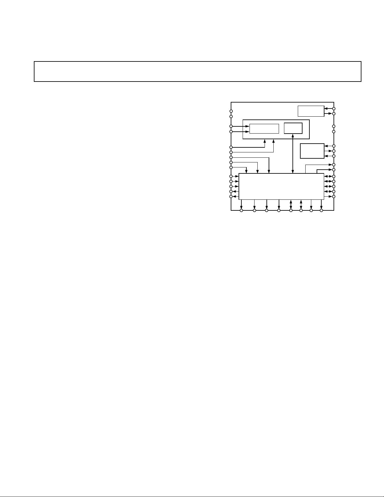
FUNCTIONAL BLOCK DIAGRAM
AGND
AV
DD
DGND
VIN(+)
VIN(–)
REF2
XTAL
CLKIN
MODE 1
STBY
SYNC
CFMT/RD
DGND/DRDY
DGND/
DB1
DOE/
DB4
SFMT/
DB5
FSI/
DB6
SCO/
DB7
MODULATOR
FIR
FILTER
XTAL
CLOCK
AD7723
DGND/
DB2
DGND/
DB3
SDO/
DB8
DGND/DB0
CONTROL
LOGIC
DV
DD
/CS
MODE 2
HALF_PWR
UNI
DGND/DB14
DGND/DB15
SCR/DB13
SLDR/DB12
SLP/DB11
TSI/DB10
FSO/DB9
XTAL_OFF
2.5V
REFERENCE
REF1
DV
DD
FEATURES
16-Bit Sigma-Delta ADC
1.2 MSPS Output Word Rate
32/16 3 Oversampling Ratio
Low-Pass and Band-Pass Digital Filter
Linear Phase
On-Chip 2.5 V Voltage Reference
Standby Mode
Flexible Parallel or Serial Interface
Crystal Oscillator
Single +5 V Supply
GENERAL DESCRIPTION
The AD7723 is a complete 16-bit, sigma-delta ADC. The part
operates from a +5␣ V supply. The analog input is continuously
sampled, eliminating the need for an external sample-and-hold.
The modulator output is processed by a finite impulse response
(FIR) digital filter. The on-chip filtering combined with a high
oversampling ratio reduces the external antialias requirements
to first order in most cases. The digital filter frequency response
can be programmed to be either low pass or band pass.
The AD7723 provides 16-bit performance for input bandwidths
up to 460␣ kHz at an output word rate up to 1.2 MHz. The
sample rate, filter corner frequencies and output word rate are
set by the crystal oscillator or external clock frequency.
Data can be read from the device in either serial or parallel
format. A stereo mode allows data from two devices to share a
single serial data line. All interface modes offer easy, high speed
connections to modern digital signal processors.
The part provides an on-chip 2.5␣ V reference. Alternatively, an
external reference can be used.
A power-down mode reduces the idle power consumption to
200 µW.
The AD7723 is available in a 44-lead PQFP package and is
specified over the industrial temperature range from –40°C to
+85°C.
Two input modes are provided, allowing both unipolar and
bipolar input ranges.
–2– REV. 0
AD7723–SPECIFICATIONS
1
B Version
Parameter Test Conditions/Comments Min Typ Max Units
DYNAMIC SPECIFICATIONS
2, 3
HALF_PWR = 0 or 1
f
CLKIN
= 10 MHz When HALF-PWR = 1
Decimate by 32
Bipolar Mode
Signal to Noise
Full Power 2.5 V Reference 87 90 dB
3 V Reference 88.5 91 dB
Half Power 86.5 89 dB
Total Harmonic Distortion
4
–96 –90 dB
Spurious Free Dynamic Range
4
2.5 V Reference –92 dB
3 V Reference –90 dB
Unipolar Mode
Signal to Noise 87 dB
Total Harmonic Distortion
4
–89 dB
Spurious Free Dynamic Range
4
–90 dB
Bandpass Filter Mode
Bipolar Mode
Signal to Noise 76 79 dB
Decimate by 16
Bipolar Mode
Signal to Noise Measurement Bandwidth = 0.383 × F
O
2.5 V Reference 82 86 dB
3 V Reference 83 87 dB
Signal to Noise Measurement Bandwidth = 0.5 × F
O
78 81.5 dB
Total Harmonic Distortion
4
2.5 V Reference –88 dB
3 V Reference –86 dB
Spurious Free Dynamic Range
4
2.5 V Reference –90 dB
3 V Reference –88 dB
Unipolar Mode
Signal to Noise Measurement Bandwidth = 0.383 × F
O
84 dB
Signal to Noise Measurement Bandwidth = 0.5 × F
O
81 dB
Total Harmonic Distortion
4
–89 dB
DIGITAL FILTER RESPONSE
Low Pass Decimate by 32
0 kHz to f
CLKIN
/83.5 ±0.001 dB
f
CLKIN
/66.9 –3 dB
f
CLKIN
/64 –6 dB
f
CLKIN
/51.9 to f
CLKIN
/2 –90 dB
Group Delay 1293/2f
CLKIN
Settling Time 1293/f
CLKIN
Low Pass Decimate by 16
0 kHz to f
CLKIN
/41.75 ±0.001 dB
f
CLKIN
/33.45 –3 dB
f
CLKIN
/32 –6 dB
f
CLKIN
/25.95 to f
CLKIN
/2 –90 dB
Group Delay 541/2f
CLKIN
Settling Time 541/f
CLKIN
Band Pass Decimate by 32
f
CLKIN
/51.90 to f
CLKIN
/41.75 ±0.001 dB
f
CLKIN
/62.95, f
CLKIN
/33.34 –3 dB
f
CLKIN
/64, f
CLKIN
/32 –6 dB
0 kHz to f
CLKIN
/83.5, f
CLKIN
/25.95 to f
CLKIN
/2 –90 dB
Group Delay 1293/2f
CLKIN
Settling Time 1293/f
CLKIN
Output Data Rate, F
O
Decimate by 32 f
CLKIN
/32
Decimate by 16 f
CLKIN
/16
ANALOG INPUTS
Full-Scale Input Span VIN(+) – VIN(–)
Bipolar Mode ±4/5 × V
REF2
V
Unipolar Mode 0 8/5 × V
REF2
V
(AV
DD
= DV
DD
= +5 V 6 5%; AGND = AGND1 = AGND2 = DGND = 0 V;
f
CLKIN
= 19.2 MHz; REF2 = 2.5 V; T
A
= T
MIN
to T
MAX
; unless otherwise noted)
–3–REV. 0
AD7723
B Version
Parameter Test Conditions/Comments Min Typ Max Units
ANALOG INPUTS (Continued)
Absolute Input Voltage VIN(+) and/or VIN(–) AGND AV
DD
V
Input Sampling Capacitance 2pF
Input Sampling Rate, f
CLKIN
19.2 MHz
CLOCK
CLKIN Duty Ratio 45 55 %
REFERENCE
REF1 Output Resistance 3kΩ
Using Internal Reference
REF2 Output Voltage 2.39 2.54 2.69 V
REF2 Output Voltage Drift 60 ppm/°C
Using External Reference
REF2 Input Impedance REF1 = AGND 4 kΩ
REF2 External Voltage Range 1.2 2.5 3.15 V
STATIC PERFORMANCE
Resolution 16 Bits
Differential Nonlinearity Guaranteed Monotonic ±0.5 ±1 LSB
Integral Nonlinearity ±2 LSB
DC CMRR 80 dB
Offset Error ±20 mV
Gain Error
5
±0.5 % FSR
LOGIC INPUTS (Excluding CLKIN)
V
INH
, Input High Voltage 2.0 V
V
INL
, Input Low Voltage 0.8 V
CLOCK INPUT (CLKIN)
V
INH
, Input High Voltage 3.8 V
V
INL
, Input Low Voltage 0.4 V
ALL LOGIC INPUTS
I
IN
, Input Current V
IN
= 0 V to DV
DD
±10 µA
C
IN
, Input Capacitance 10 pF
LOGIC OUTPUTS
V
OH
, Output High Voltage |I
OUT
| = 200 µA 4.0 V
V
OL
, Output Low Voltage |I
OUT
| = 1.6 mA 0.4 V
POWER SUPPLIES
AV
DD
4.75 5.25 V
I
AVDD
HALF_PWR = Logic Low 50 60 mA
HALF_PWR = Logic High 25 33 mA
DV
DD
4.75 5.25 V
I
DVDD
HALF_PWR = Logic Low 25 35 mA
HALF_PWR = Logic High 15 20 mA
Power Consumption
6
Standby Mode 200 µW
NOTES
1
Operating temperature range is as follows: B Version: –40°C to +85°C.
2
Typical values for SNR apply for parts soldered directly to a printed circuit board ground plane.
3
Dynamic specifications apply for input signal frequencies from dc to 0.0240 × f
CLKIN
in decimate by 16 mode and from dc to 0.0120 × f
CLKIN
in decimate by 32 mode.
4
When using the internal reference, THD and SFDR specifications apply only to input signals above 10 kHz with a 10 µF decoupling capacitor between REF2 and
AGND2. At frequencies below 10 kHz, THD degrades to 84 dB and SFDR degrades to 86 dB.
5
Gain Error excludes Reference Error.
6
CLKIN and digital inputs static and equal to 0 or DV
DD
.
Specifications subject to change without notice.
AD7723
–4– REV. 0
(AV
DD
= DV
DD
= +5 V 6 5%; AGND = AGND1 = DGND = 0 V; f
CLKIN
= 19.2 MHz; C
L
= 50 pF; SFMT =
Logic Low or High, CFMT = Logic Low or High; T
A
= T
MIN
to T
MAX
unless otherwise noted)
TIMING SPECIFICATIONS
Parameter Symbol Min Typ Max Units
CLKIN Frequency F
CLK
1 19.2 MHz
CLKIN Period (t
CLK
= 1/f
CLK
)t
1
0.052 1 µs
CLKIN Low Pulsewidth t
2
0.45 × t
1
0.55 × t
1
CLKIN High Pulsewidth t
3
0.45 × t
1
0.55 × t
1
CLKIN Rise Time t
4
5ns
CLKIN Fall Time t
5
5ns
FSI Setup Time t
6
05ns
FSI Hold Time t
7
05ns
FSI High Time
1
t
8
1t
CLK
CLKIN to SCO Delay t
9
25 40 ns
SCO Period
2
, SCR = 1 t
10
2t
CLK
SCO Period
2
, SCR = 0 t
10
1t
CLK
SCO Transition to FSO High Delay t
11
05 ns
SCO Transition to FSO Low Delay t
12
05 ns
SCO Transition to SDO Valid Delay t
13
512 ns
SCO Transition from FSI
3
t
14
60 t
CLK
+ t
2
SDO Enable Delay Time t
15
520 ns
SDO Disable Delay Time t
16
520 ns
DRDY High Time
2
t
17
2t
CLK
Conversion Time
2
(Refer to Tables I and II) t
18
16/32 t
CLK
CLKIN to DRDY Transition t
19
35 50 ns
CLKIN to DATA Valid t
20
20 35 ns
CS/RD Setup Time to CLKIN t
21
0ns
CS/RD Hold Time to CLKIN t
22
20 ns
Data Access Time t
23
20 35 ns
Bus Relinquish Time t
24
20 35 ns
SYNC Input Pulsewidth t
25
1t
CLK
SYNC Low Time before CLKIN Rising t
26
0ns
DRDY High Delay after Rising SYNC t
27
25 35 ns
DRDY Low Delay after SYNC Low t
28
2049 t
CLK
NOTES
1
FSO pulses are gated by the release of FSI (going low).
2
Guaranteed by design.
3
Frame Sync is initiated on the falling edge of CLKIN.
Specifications subject to change without notice.
I
OL
1.6mA
+1.6V
C
L
50pF
TO
OUTPUT
PIN
I
OH
200mA
Figure 1. Load Circuit for Timing Specifications
AD7723
–5–REV. 0
CLKIN
FSI
SCO
2.3V
t
4
t
5
t
7
t
6
t
9
t
3
t
2
t
1
t
10
t
9
t
8
0.8V
Figure 2. Serial Mode Timing for Clock Input, Frame Sync Input and Serial Clock Output
CLKIN
FSI
(SFMT = 1)
SCO
(CFMT = 0)
FSO
(SFMT = 0)
FSO
(SFMT = 1)
SDO
32 CLKIN CYCLES
t
8
t
11
t
12
t
13
t
14
t
11
D15 D14 D13 D2 D1 D0 D15 D14
Figure 3. Serial Mode 1. Timing for Frame Sync Input, Frame Sync Output, Serial Clock Output and Serial Data Output
(Refer to Table I for Control Inputs, TSI = DOE)
D2 D1 D0 D15 D14 D13 D12 D11
D5
D4
D3 D2 D1 D0 D15 D14
t
8
t
11
t
12
t
13
t
14
32 CLKIN CYCLES
CLKIN
FSI
SCO
(CFMT = 0)
FSO
SDO
Figure 4. Serial Mode 2. Timing for Frame Sync Input, Frame Sync Output, Serial Clock Output and Serial Data Output
(Refer to Table I for Control Inputs, TSI = DOE)
剩余22页未读,继续阅读
资源评论
书博教育
- 粉丝: 1
- 资源: 2836
上传资源 快速赚钱
- 我的内容管理 展开
- 我的资源 快来上传第一个资源
- 我的收益 登录查看自己的收益
- 我的积分 登录查看自己的积分
- 我的C币 登录后查看C币余额
- 我的收藏
- 我的下载
- 下载帮助
安全验证
文档复制为VIP权益,开通VIP直接复制
信息提交成功