没有合适的资源?快使用搜索试试~ 我知道了~
AP162401-芯片资料介绍.PDF
1.该资源内容由用户上传,如若侵权请联系客服进行举报
2.虚拟产品一经售出概不退款(资源遇到问题,请及时私信上传者)
版权申诉
0 下载量 15 浏览量
2022-07-04
11:03:42
上传
评论
收藏 198KB PDF 举报
温馨提示
试读
16页
AP162401-芯片资料介绍.PDF
资源推荐
资源详情
资源评论
Semiconductor Group 1.97, Rel. 01
Microcontrollers
ApNote AP1624
þ
additional file
AP162401.EXE available
Software emulation of the I
2
C-bus using the General
Purpose Timer unit 1 of the C166 family
This is a software emulation of the I
2
C-bus by using two general purpose timers of a
microcontroller from the C166 family. The I
2
C-bus is used in many applications mainly
to communicate between devices connected to the bus.
Author: Tan Choon Hock / SCPL HL RM LAB
Software emulation of the I
2
C-bus using the
General Purpose Timer unit 1 of the 166 family
Semiconductor Group of 16 AP1624 1.97
2
1 Introduction to I
2
C-bus ................................................................................................ 3
2 I
2
C-bus Specifications ................................................................................................. 3
2.1 Data Transfer Formats................................................................................................. 3
2.2 Timing Diagram............................................................................................................ 6
2.3 Hardware Connection .................................................................................................. 8
3 Software Description.................................................................................................... 9
3.1 Software Concept......................................................................................................... 9
3.2 Description of Module Subroutines............................................................................ 10
3.3 Software Compilation................................................................................................. 15
AP1624 ApNote - Revision History
Actual Revision : Rel. 01 Previous Revision: none (Original Version)
Page of
actual Rel.
Page of
prev. Rel.
Software emulation of the I
2
C-bus using the
General Purpose Timer unit 1 of the 166 family
Semiconductor Group of 16 AP1624 1.97
3
1 Introduction to I
2
C-bus
The I
2
C-bus or Inter-Integrated Circuit bus has been developed by Philips. It allows
integrated circuits to communicate directly with each other via a simple bi-directional 2-
wire bus. The two bus lines are serial clock line (SCL), and serial data line (SDA).
Nowadays, the I
2
C-bus becomes a standard bus system which is used in consumer
electronics, telecommunications, and industrial electronics. This software module for I
2
C-
bus emulation supports the single master protocol only. It is using a timer interrupt to
generate clock and transmit or receive the data. The clock frequency of the I
2
C-bus can
achieve up to 100 KHz with 20 MHz CPU of the C16x microcontroller.
2 I
2
C-bus Specification
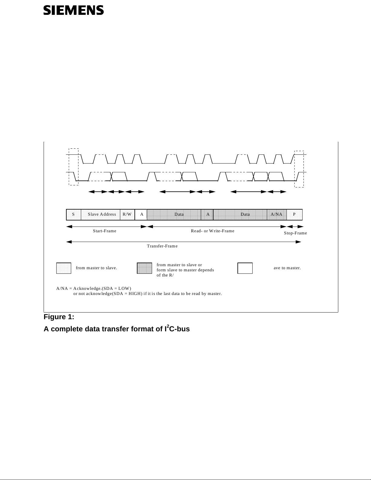
2.1 Data Transfer formats
A HIGH-to-LOW transition of the data line (SDA) while the clock line (SCL) is HIGH
indicates a START condition. A LOW-to-HIGH transition of the SDA while SCL is HIGH
defines a STOP condition. The data line can only be changed when the clock signal on
the SCL line is LOW. Therefore, the data on the SDA line must be stable during the HIGH
period of the clock signal. The bus is considered to be busy after the START condition
and is considered to be free at a certain time interval after the STOP condition.
Each information put on the SDA line must be 8-bit long. The data is transferred serially
with the most significant bit first, and followed by an acknowledge bit. The 9th clock pulse
of the acknowledge bit is generated by the master. The transmitting device has to release
the SDA line (HIGH or in the high impedance state) during this clock pulse while the
device that needs to acknowledge has to pull down the SDA line during this clock pulse.
The number of data bytes transferred between the START and STOP condition from the
transmitter and receiver is not limited.
The receiver is obliged to generate an acknowledge bit after each byte of data that has
been received. When the receiver does not provide an acknowledge bit after having
received a byte of data, the data line must be left HIGH or in the high impedance state by
the slave. The master can then generate a STOP condition to abort the transfer. One of
the reasons for the receiver not to provide the acknowledge bit is that the receiver is
performing some real- time function. If the master is receiving data, it must signal the end
of the data to the slave by not generating an acknowledge bit on the last byte of data
received. Then, the slave must release the data line to allow the master to generate the
STOP condition.
Software emulation of the I
2
C-bus using the
General Purpose Timer unit 1 of the 166 family
Semiconductor Group of 16 AP1624 1.97
4
A complete data transfer format is shown in Figure #1. After a START condition, a slave
address is sent. The address is 7 bits long followed by an 8th bit which is a data direction
bit (R/W). A “0” for data direction bit indicates a transmission (WRITE), and a “1”
indicates a request for data (READ). Figure #2 shows the I
2
C-bus data transfer format of
writing data from master to slave device. Figure #3 shows the data transfer format of
reading data from the slave device.
A data transfer is always terminated by a STOP condition generated by the master.
However, if the master still wishes to communicate on the bus, it can generate a repeated
START condition and address the same device or another slave device without first
generating a STOP condition. This combined data transfer format is shown in figure #4.
Start
Condition
SDA
SCL
1-7 89 891-7 891-7
Stop
Condition
Address
R/W
Ack
Data Ack Data Ack
AAAA
A
AAA
A
AAA
A
AAA
A
AAA
AAAA
AAAA
AAA
A
AAA
A
AAA
A
AAA
A
AAAA
S
AAAA
A
AAA
A
AAA
A
AAA
A
AAA
AAAA
AAAA
AAAA
AAAA
AAAA
AAAA
AAAA
AAAA
AAAA
AAAA
AAAA
AAAA
AAAA
AAAA
AAAA
AAAA
AAAA
AAAA
AAAA
AAAA
AAA
A
AAA
A
AAA
A
AAA
A
AAAA
Slave Address
AAAA
A
AAA
A
AAA
A
AAA
A
AAA
AAAA
AAAA
AAA
A
AAA
A
AAA
A
AAA
A
AAAA
R/W A
AAAA
AAAA
AAAA
AAAA
AAAA
AAAA
AAAA
AAAA
AAAA
AAAA
AAAA
AAAA
AAAA
AAAA
AAAA
AAAA
AAAA
AAAA
AAAA
AAAA
AAAA
AAAA
AAAA
AAAA
AAAA
AAAA
AAAA
AAAA
AAAA
AAAA
AAAA
AAAA
AAAA
AAAA
AAAA
AAAA
AAAA
AAAA
AAAA
AAAA
AAAA
AAAA
A
A
A
A
A
A
Data
AAAA
A
AAA
A
AAA
A
AAA
A
AAA
AAAA
AAA
AA
A
AA
A
AA
A
AA
A
AAA
A
AAAA
AAAA
AAAA
AAAA
AAAA
AAAA
AAAA
AAAA
AAAA
AAAA
AAAA
AAAA
AAAA
AAAA
AAAA
AAAA
AAAA
AAAA
AAAA
AAAA
AAAA
AAAA
AAAA
AAAA
AAAA
AAAA
AAAA
AAAA
AAAA
AAAA
AAAA
AAAA
AAAA
AAAA
AAAA
AAAA
AAAA
AAAA
AAAA
AAAA
AAAA
AAAA
A
A
A
A
A
A
Data
AAAA
A
AAA
A
AAA
A
AAA
A
AAA
AAAA
AAAA
AAAA
AAAA
AAAA
AAAA
AAAA
AA
A
A
A
A
A
A
A
A
AA
A/NA
AAAA
AAAA
AAAA
AAAA
AAAA
AAAA
AAAA
AAA
A
AAA
A
AAA
A
AAA
A
AAAA
P
Start-Frame Read- or Write-Frame
Stop-Frame
Transfer-Frame
AAAA
A
AAA
A
AAA
A
AAA
A
AAA
AAAA
AAAA
AAA
A
AAA
A
AAA
A
AAA
A
AAAA
AAAA
AAAA
AAAA
AAAA
AAAA
AAAA
AAA
AA
A
AA
A
AA
A
AA
A
AAA
from master to slave.
from master to slave or
form slave to master depends
of the R/W bit.
from slave to master.
A/NA = Acknowledge.(SDA = LOW)
or not acknowledge(SDA = HIGH) if it is the last data to be read by master.
Figure 1:
A complete data transfer format of I
2
C-bus
剩余15页未读,继续阅读
资源评论
书博教育
- 粉丝: 1
- 资源: 2836
上传资源 快速赚钱
- 我的内容管理 展开
- 我的资源 快来上传第一个资源
- 我的收益 登录查看自己的收益
- 我的积分 登录查看自己的积分
- 我的C币 登录后查看C币余额
- 我的收藏
- 我的下载
- 下载帮助
安全验证
文档复制为VIP权益,开通VIP直接复制
信息提交成功