没有合适的资源?快使用搜索试试~ 我知道了~
AD694-芯片资料介绍.PDF
1.该资源内容由用户上传,如若侵权请联系客服进行举报
2.虚拟产品一经售出概不退款(资源遇到问题,请及时私信上传者)
版权申诉
0 下载量 182 浏览量
2022-07-04
11:16:56
上传
评论
收藏 427KB PDF 举报
温馨提示
试读
12页
AD694-芯片资料介绍.PDF
资源推荐
资源详情
资源评论
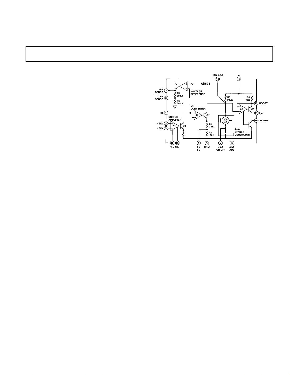
FUNCTIONAL BLOCK DIAGRAM
REV. A
Information furnished by Analog Devices is believed to be accurate and
reliable. However, no responsibility is assumed by Analog Devices for its
use, nor for any infringements of patents or other rights of third parties
which may result from its use. No license is granted by implication or
otherwise under any patent or patent rights of Analog Devices.
a
4–20 mA Transmitter
AD694*
FEATURES
4–20 mA, 0–20 mA Output Ranges
Precalibrated Input Ranges:
0 V to 2 V, 0 V to 10 V
Precision Voltage Reference
Programmable to 2.000 V or 10.000 V
Single or Dual Supply Operation
Wide Power Supply Range: +4.5 V to +36 V
Wide Output Compliance
Input Buffer Amplifier
Open-Loop Alarm
Optional External Pass Transistor to Reduce
Self-Heating Errors
0.002% typ Nonlinearity
PRODUCT DESCRIPTION
The AD694 is a monolithic current transmitter that accepts
high level signal inputs to drive a standard 4–20 mA current
loop for the control of valves, actuators, and other devices com-
monly used in process control. The input signal is buffered by
an input amplifier that can be used to scale the input signal or
buffer the output from a current mode DAC. Precalibrated in-
put spans of 0 V to 2 V and 0 V to 10 V are selected by simple
pin strapping; other spans may be programmed with external
resistor.
The output stage compliance extends to within 2 V of V
S
and its
special design allows the output voltage to extend below com-
mon in dual supply operation. An alarm warns of an open 4-to-
20 mA loop or noncompliance of the output stage.
Active laser trimming of the AD694’s thin film resistors results
in high levels of accuracy without the need for additional adjust-
ments and calibration. An external pass transistor may be used
with the AD694 to off-load power dissipation, extending the
temperature range of operation.
The AD694 is the ideal building block for systems requiring
noise immune 4–20 mA signal transmission to operate valves,
actuators, and other control devices, as well as for the transmis-
sion of process parameters such as pressure, temperature, or
flow. It is recommended as a replacement for discrete designs in
a variety of applications in industrial process control, factory
automation, and system monitoring.
The AD694 is available in hermetically sealed, 16-pin cerdip
and plastic SOIC, specified over the –40°C to +85°C industrial
temperature range, and in a 16-pin plastic DIP, specified over
the 0°C to +70°C temperature range.
*Protected by U.S. Patents: 30,586; 4,250,445; 4,857,862.
One Technology Way, P.O. Box 9106, Norwood, MA 02062-9106, U.S.A.
Tel: 617/329-4700 Fax: 617/326-8703
PRODUCT HIGHLIGHTS
1. The AD694 is a complete voltage in to 4–20 mA out current
transmitter.
2. Pin programmable input ranges are pre-calibrated at 0 V to
2 V and 0 V to 10 V.
3. The input amplifier may be configured to buffer and scale the
input voltage, or to serve as an output amplifier for current
output DACs.
4. The output voltage compliance extends to within 2 V of the
positive supply and below common. When operated with a
5 V supply, the output voltage compliance extends 30 V be-
low common.
5. The AD694 interfaces directly to 8-, 10-, and 12-bit single
supply CMOS and bipolar DACs.
6. The 4 mA zero current may be switched on and off with a
TTL control pin, allowing 0–20 mA operation.
7. An open collector alarm warns of loop failure due to open
wires or noncompliance of the output stage.
8. A monitored output is provided to drive an external pass
transistor. The feature off-loads power dissipation to extend
the temperature range of operation and minimize self-heating
error.
AD694–SPECIFICATIONS
Model AD694JN/AQ/AR AD694BQ/BR
Min Typ Max Min Typ Max Units
INPUT CHARACTERISTICS
Input Voltage Range –0.2 V
S
–2.0 V V
S
–2.5 V –0.2 V
S
–2.0 V V
S
–2.5 V V
Input Bias Current
Either Input, T
MIN
to T
MAX
1.5 5 1.5 5 nA
Offset Current, T
MIN
to T
MAX
±0.1 61 ±0.1 61 nA
Offset Current Drift ±1.0 ±5.0 ±1.0 ±5.0 pA/°C
Input Impedance 5 5 MΩ
OUTPUT CHARACTERISTICS
Operating Current Range 0 23 0 23 mA
Specified Performance 4 20 4 20 mA
Output Voltage Compliance V
S
–36 V V
S
–2 V V
S
–36 V V
S
–2 V V
Output Impedance, 4–20 mA 40.0 50.0 40.0 50.0 MΩ
Current Limit (@ 2 × FS Overdrive 24 44 24 44 mA
Slew Rate 1.3 1.3 mA/µs
SPAN AND ZERO ACCURACY
1
4 mA Offset Error @ 0 V Input
2
Error from 4.000 mA, 4 mA On ±10 620 ±5 610 µA
Error from 0.000 mA, 4 mA Off 0 +10 +20 0+5+10 µA
T
MIN
to T
MAX
±10 640 ±5 620 µA
vs. Supply (2 V Span/10 V Span) 0.3/0.05 0.8/0.4 0.3/0.05 0.8/0.4 µA/V
Trim Range, 4 mA Zero 2.0 4.8 2.0 4.8 mA
Span
Nominal Transfer Function
Input FS = 2 V 8.0 8.0 mA/V
Input FS = 10 V 1.6 1.6 mA/V
Transfer Function Error from Nom,
Input FS = 2 V, 10 V ±0.1 60.3 ±0.05 60.15 % of Span
T
MIN
to T
MAX
±0.002 ±0.005 ±0.001 60.0025 % of Span/°C
vs. Supply ±0.001 60.005 ±0.001 60.005 % of Span/V
Nonlinearity
3
±0.005 60.015 ±0.001 60.005 % of Span
4 mA On: Max Pin 9 Voltage 0.8 0.8 V
4 mA Off: Min Pin 9 Voltage 3.0 2.5 3.0 2.5 V
VOLTAGE REFERENCE
Output Voltage: 10 V Reference 9.960 10.000 10.040 9.980 10.000 10.020 V
Output Voltage: 2 V Reference 1.992 2.000 2.008 1.996 2.000 2.004 V
T
MIN
to T
MAX
4
30 50 20 30 ppm/°C
vs. Load, V
REF
= 2 V, 10 V 0.15 0.50 0.15 0.50 mV/mA
vs. Supply, V
REF
= 2 V, 10 V ±0.001 60.005 ±0.001 60.005 %/V
Output Current
Source 5 5mA
Sink 0.2 0.2 mA
ALARM CHARACTERISTICS
V
CE(SAT)
@ 2.5 mA 0.35 0.35 V
Leakage Current 61 61 µA
Alarm Pin Current (Pin 10) 20 20 mA
POWER REQUIREMENTS
Specified Performance 24 24 V
Operating Range
2 V FS, V
REF
= 2 V 4.5 36 4.5 36 V
2 V, 10 V FS, V
REF
= 2 V, 10 V 12.5 36 12.5 36 V
Quiescent Current, 4 mA Off 1.5 2.0 1.5 2.0 mA
TEMPERATURE RANGE
Specified Performance
5
AD694AQ/BQ/AR/BR –40 +85 –40 +85 °C
AD694JN 0 +70 0 +70 °C
Operating AD694AQ/BQ/AR/BR –55 +125 –55 +125 °C
AD694JN –40 +85 –40 +85 °C
(@ +258C, R
L
= 250 V and V
S
= +24 V, unless otherwise noted)
REV. A
–2–
Model AD694JN/AQ/AR AD694BQ/BR
Min Typ Max Min Typ Max Units
BUFFER AMPLIFIER
6
Input Offset Voltage
Initial Offset ±150 6500 ±50 6500 µV
T
MIN
to T
MAX
±2 ±3 ±2 ±3 µV/°C
vs. Supply 80 90 80 90 dB
vs. Common Mode 80 90 80 90 dB
Trim Range 62.5 ±4.0 62.5 ±4.0 mV
Frequency Response
Unity Gain, Small Signal 300 300 kHz
Input Voluge Noise (0.1 Hz to 10 Hz) 2 2 µV p-p
Open-Loop Gain
V
O
= +10 V, R
L
≥ 10 kΩ 50 50 V/mV
Output Voltage @ Pin 1, FB
1
Minimum Output Voltage 1.0 10 1.0 10 mV
Maximum Output Voltage V
S
–2.5 V V
S
–2 V V
S
–2.5 V V
S
–2 V V
NOTES
1
The single supply op amps of the AD694, lacking pull down current, may not reach 0.000 V at their outputs. For this reason, span, offset, and nonlinearity are
specified with the input amplifiers operating in their linear range. The input voltage used for the tests is 5 mV to 2 V and 5 mV to 10 V for the two precalibrated
input ranges. Span and zero accuracy are tested with the buffer amplifier configured as a follower.
2
Offset at 4 mA out and 0 mA out are extrapolated to 0.000 V input from measurements made at 5 mV and at full scale. See Note 1.
3
Nonlinearity is specified as the maximum deviation of the output, as a % of span, from a straight line drawn through the endpoints of the transfer function.
4
Voltage reference drift guaranteed by the Box Method. The voltage reference output over temperature will fall inside of a box whose length is determined by the
temperature range and whose height is determined by the maximum temperature coefficient multiplied by the temperature span in degrees C.
5
Devices tested at these temperatures with a pass transistor. Allowable temperature range of operation is dependent upon internal power dissipation. Absolute
maximum junction and case temperature should not be exceeded. See section: “Power Dissipation Considerations.”
6
Buffer amplifier specs for reference. Buffer amplifier offset and drift already included in Span and Zero accuracy specs above.
Specifications subject to change without notice.
PIN CONFIGURATION (N, R, Q PACKAGE)
AD694
REV. A
–3–
ABSOLUTE MAXIMUM RATINGS
Supply Voltage . . . . . . . . . . . . . . . . . . . . . . . . . . . . . . . . +36 V
V
S
to I
OUT
. . . . . . . . . . . . . . . . . . . . . . . . . . . . . . . . . . . +36 V
Input Voltage, (Either Input Pin 2 or 3) . . . . .–0.3 V to +36 V
Reference Short Circuit to Common . . . . . . . . . . . . Indefinite
Alarm Voltage, Pin 10 . . . . . . . . . . . . . . . . . . . . . . . . . . +36 V
4 mA Adj, Pin 6 . . . . . . . . . . . . . . . . . . . . . . . . . . . . . . . . +1 V
4 mA On/Off, Pin 9 . . . . . . . . . . . . . . . . . . . . . . . . 0 V to 36 V
Storage Temperature Range
AD694Q . . . . . . . . . . . . . . . . . . . . . . . . . –65°C to +150°C
AD694N, R . . . . . . . . . . . . . . . . . . . . . . . –65°C to +125°C
Lead Temperature, 10 sec Soldering . . . . . . . . . . . . . . +300°C
Maximum Junction Temperature . . . . . . . . . . . . . . . . . +150°C
Maximum Case Temperature
Plastic Package (N, R) . . . . . . . . . . . . . . . . . . . . . . . +125°C
Cerdip Package (Q) . . . . . . . . . . . . . . . . . . . . . . . . . +125°C
No pin, other than I
OUT
(11) and ±Sig (2), (3) as noted, may be permitted to become more negative than Com (5). No pin may be
permitted to become more positive than V
S
(13).
ORDERING GUIDE
Temperature Package
Model Range Option*
AD694JN 0°C to +70°C N-16
AD694AQ –40°C to +85°C Q-16
AD694AR –40°C to +85°C R-16
AD694BQ –40°C to +85°C Q-16
AD694BR –40°C to +85°C R-16
*N = Plastic DIP; Q = Cerdip, R = SOIC.
Transistor Count: . . . . . . . . . . . . . . . . . . . . .75 Active Devices
Substrate Connection: . . . . . . . . . . . . . . . . . . . . to Com, Pin 5
Thermal Characteristics:
Plastic (N) Package: θ
JC
= 50°C/Watt
θ
CA
(Still Air) = 85°C/Watt
Cerdip (Q) Package: θ
JC
= 30°C/Watt
θ
CA
(Still Air) = 70°C/Watt
Plastic (R) Package: θ
JC
= 27°C/Watt
θ
CA
(Still Air) = 73°C/Watt
ESD Susceptibility
All pins are rated for a minimum of 4000 V protection, except
for Pins 2, 3 and 9 which are rated to survive a minimum of
1500 V. ESD testing conforms to Human Body Model. Always
practice ESD prevention.
剩余11页未读,继续阅读
资源评论
书博教育
- 粉丝: 1
- 资源: 2837
上传资源 快速赚钱
- 我的内容管理 展开
- 我的资源 快来上传第一个资源
- 我的收益 登录查看自己的收益
- 我的积分 登录查看自己的积分
- 我的C币 登录后查看C币余额
- 我的收藏
- 我的下载
- 下载帮助
最新资源
- 微信小程序源码 车源宝 二手车交易平台 源码下载
- 微信小程序源码 实现 城市切换 demo 根据城市首字母排序城市 选择城市 源码下载
- VMware7.0虚拟机硬盘无法编辑,无法连接到Profile-Driven Storage Service
- arm64内核的mongo镜像
- 基于stm32f103c单片机+MPU6050+0.96英寸OLED显示屏双柄遥控器硬件(原理图+PCB)工程文件.zip
- 整理的关于少儿编程的学习路径,以及如何在小升初,初升高和大学充分的利用起来编程经验的优势
- nhit完整源码+论文学习
- 足球比赛结果统计表2006-2011年大约28W场比赛
- 基于PHP+mysql的社区交流系统(源代码)
- yolov5,SSD 可能使用到的一些代码
资源上传下载、课程学习等过程中有任何疑问或建议,欢迎提出宝贵意见哦~我们会及时处理!
点击此处反馈
安全验证
文档复制为VIP权益,开通VIP直接复制
信息提交成功