没有合适的资源?快使用搜索试试~ 我知道了~
AD811-芯片资料介绍.pdf
1.该资源内容由用户上传,如若侵权请联系客服进行举报
2.虚拟产品一经售出概不退款(资源遇到问题,请及时私信上传者)
版权申诉
0 下载量 14 浏览量
2022-07-04
11:15:22
上传
评论
收藏 242KB PDF 举报
温馨提示
试读
15页
AD811-芯片资料介绍.pdf
资源推荐
资源详情
资源评论
a
High Performance
Video Op Amp
AD811
One Technology Way, P.O. Box 9106, Norwood, MA 02062-9106, U.S.A.
Tel: 781/329-4700 World Wide Web Site: http://www.analog.com
Fax: 781/326-8703 © Analog Devices, Inc., 1999
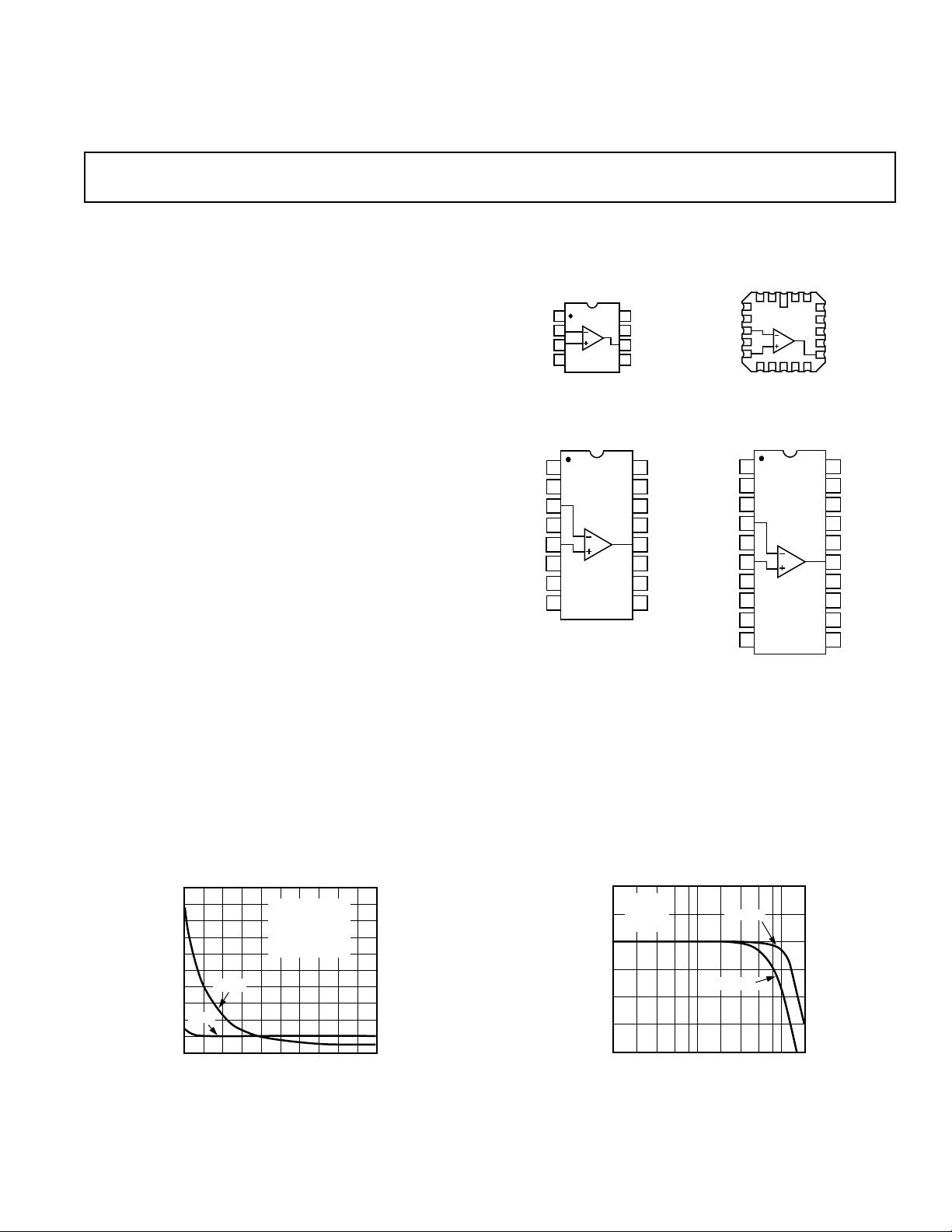
CONNECTION DIAGRAMS
FEATURES
High Speed
140 MHz Bandwidth (3 dB, G = +1)
120 MHz Bandwidth (3 dB, G = +2)
35 MHz Bandwidth (0.1 dB, G = +2)
2500 V/s Slew Rate
25 ns Settling Time to 0.1% (For a 2 V Step)
65 ns Settling Time to 0.01% (For a 10 V Step)
Excellent Video Performance (R
L
=150 ⍀)
0.01% Differential Gain, 0.01ⴗ Differential Phase
Voltage Noise of 1.9 nV√Hz
Low Distortion: THD = –74 dB @ 10 MHz
Excellent DC Precision
3 mV max Input Offset Voltage
Flexible Operation
Specified for ⴞ5 V and ⴞ15 V Operation
ⴞ2.3 V Output Swing into a 75 ⍀ Load (V
S
= ⴞ5 V)
APPLICATIONS
Video Crosspoint Switchers, Multimedia Broadcast
Systems
HDTV Compatible Systems
Video Line Drivers, Distribution Amplifiers
ADC/DAC Buffers
DC Restoration Circuits
Medical—Ultrasound, PET, Gamma and Counter
Applications
The AD811 is also excellent for pulsed applications where tran-
sient response is critical. It can achieve a maximum slew rate of
greater than 2500 V/µs with a settling time of less than 25 ns to
0.1% on a 2 volt step and 65 ns to 0.01% on a 10 volt step.
The AD811 is ideal as an ADC or DAC buffer in data acquisi-
tion systems due to its low distortion up to 10 MHz and its wide
unity gain bandwidth. Because the AD811 is a current feedback
amplifier, this bandwidth can be maintained over a wide range
of gains. The AD811 also offers low voltage and current noise of
1.9 nV/√Hz and 20 pA/√Hz, respectively, and excellent dc accu-
racy for wide dynamic range applications.
12
–6
3
–3
0
1M
9
6
10M 100M
FRE
QU
EN
C
Y – Hz
GAIN – dB
G = +2
R
L
= 150V
R
G
= R
FB
V
S
= 65V
V
S
= 615V
PRODUCT DESCRIPTION
The AD811 is a wideband current-feedback operational ampli-
fier, optimized for broadcast quality video systems. The –3 dB
bandwidth of 120 MHz at a gain of +2 and differential gain and
phase of 0.01% and 0.01° (R
L
= 150 Ω) make the AD811 an
excellent choice for all video systems. The AD811 is designed to
meet a stringent 0.1 dB gain flatness specification to a band-
width of 35 MHz (G = +2) in addition to the low differential
gain and phase errors. This performance is achieved whether
driving one or two back terminated 75 Ω cables, with a low
power supply current of 16.5 mA. Furthermore, the AD811 is
specified over a power supply range of ±4.5 V to ±18 V.
0.10
15
0.03
0.01
6
0.02
5
0.06
0.04
0.05
0.07
0.08
0.09
1413121110987
0.20
0.18
0.16
0.14
0.12
0.10
0.08
0.06
0.04
0.02
SUPPLY VOLTAGE –
6
Volts
DIFFERENTIAL GAIN –
%
DIFFERENTIAL PHASE – Degrees
R
F
= 649V
F
C
= 3.58MHz
100 IRE
MODULATED RAMP
R
L
= 150V
GAIN
PHASE
16-Lead SOIC (R-16) Package 20-Lead SOIC (R-20) Package
+IN
NC
+V
S
1
2
3
4
5
6
7
8
16
15
14
13
12
11
10
9
AD811
NC
–IN
NC
+IN
–V
S
NC
NC
NC
NC
OUTPUT
NC
NC
NC = NO CONNECT
3
4
5
6
7
8
9
10
18
17
16
15
14
13
12
11
AD811
NC
–IN
NC
NC
–V
S
NC
NC
NC
+V
S
NC
OUTPUT
NC
NC
NC = NO CONNECT
NC
NC
1
2
20
19
NC
NC
NC
NC
NC
NC
20-Lead LCC (E-20A) Package
REV. D
Information furnished by Analog Devices is believed to be accurate and
reliable. However, no responsibility is assumed by Analog Devices for its
use, nor for any infringements of patents or other rights of third parties
which may result from its use. No license is granted by implication or
otherwise under any patent or patent rights of Analog Devices.
1
2
3
4
8
7
6
5
AD811
32
1
20
19
18
17
16
15
14
9
10 11
12 13
4
5
6
7
8
AD811
NC
NC
+V
S
NC
OUTPUT
–V
S
NC
NC
NC
NC
–IN
+IN
NC
NC
NC
NC
NC
NC
–IN
+IN
–V
S
NC
OUTPUT
NC
+V
S
NC = NO CONNECT
NC = NO CONNECT
NC
NC
NC
8-Lead Plastic (N-8)
Cerdip (Q-8)
SOIC (SO-8) Packages
AD811J/A
1
AD811S
2
Model Conditions V
S
Min Typ Max Min Typ Max Units
DYNAMIC PERFORMANCE
Small Signal Bandwidth (No Peaking)
–3 dB
G = +1 R
FB
= 562 Ω±15 V 140 140 MHz
G = +2 R
FB
= 649 Ω±15 V 120 120 MHz
G = +2 R
FB
= 562 Ω±5 V 80 80 MHz
G = +10 R
FB
= 511 Ω±15 V 100 100 MHz
0.1 dB Flat
G = +2 R
FB
= 562 Ω±5 V 25 25 MHz
R
FB
= 649 Ω±15 V 35 35 MHz
Full Power Bandwidth
3
V
OUT
= 20 V p-p ±15 V 40 40 MHz
Slew Rate V
OUT
= 4 V p-p ±5 V 400 400 V/µs
V
OUT
= 20 V p-p ±15 V 2500 2500 V/µs
Settling Time to 0.1% 10 V Step, A
V
= –1 ±15 V 50 50 ns
Settling Time to 0.01% 65 65 ns
Settling Time to 0.1% 2 V Step, A
V
= –1 ±5 V 25 25 ns
Rise Time, Fall Time R
FB
= 649, A
V
= +2 ±15 V 3.5 3.5 ns
Differential Gain f = 3.58 MHz ±15 V 0.01 0.01 %
Differential Phase f = 3.58 MHz ±15 V 0.01 0.01 Degree
THD @ f
C
= 10 MHz V
OUT
= 2 V p-p, A
V
= +2 ±15 V –74 –74 dBc
Third Order Intercept
4
@ f
C
= 10 MHz ±5 V 36 36 dBm
±15 V 43 43 dBm
INPUT OFFSET VOLTAGE ±5 V, ±15 V 0.5 3 0.5 3 mV
T
MIN
to T
MAX
55mV
Offset Voltage Drift 55µV/°C
INPUT BIAS CURRENT
–Input ±5 V, ±15 V 2 5 2 5 µA
T
MIN
to T
MAX
15 30 µA
+Input ±5 V, ±15 V 2 10 2 10 µA
T
MIN
to T
MAX
20 25 µA
TRANSRESISTANCE T
MIN
to T
MAX
V
OUT
= ±10 V
R
L
= ∞±15 V 0.75 1.5 0.75 1.5 MΩ
R
L
= 200 Ω±15 V 0.5 0.75 0.5 0.75 MΩ
V
OUT
= ±2.5 V
R
L
= 150 Ω±5 V 0.25 0.4 0.125 0.4 MΩ
COMMON-MODE REJECTION
V
OS
(vs. Common Mode)
T
MIN
to T
MAX
V
CM
= ±2.5 ±5 V 56 60 50 60 dB
T
MIN
to T
MAX
V
CM
= ±10 V ±15 V 60 66 56 66 dB
Input Current (vs. Common Mode) T
MIN
to T
MAX
13 1 3µA/V
POWER SUPPLY REJECTION V
S
= ±4.5 V to ±18 V
V
OS
T
MIN
to T
MAX
60 70 60 70 dB
+Input Current T
MIN
to T
MAX
0.3 2 0.3 2 µA/V
–Input Current T
MIN
to T
MAX
0.4 2 0.4 2 µA/V
INPUT VOLTAGE NOISE f = 1 kHz 1.9 1.9 nV/√Hz
INPUT CURRENT NOISE f = 1 kHz 20 20 pA/√Hz
OUTPUT CHARACTERISTICS
Voltage Swing, Useful Operating Range
5
±5 V ±2.9 ±2.9 V
±15 V ±12 ±12 V
Output Current T
J
= +25°C 100 100 mA
Short-Circuit Current 150 150 mA
Output Resistance (Open Loop @ 5 MHz) 9 9 Ω
INPUT CHARACTERISTICS
+Input Resistance 1.5 1.5 MΩ
–Input Resistance 14 14 Ω
Input Capacitance +Input 7.5 7.5 pF
Common-Mode Voltage Range ±5 V ±3 ±3V
±15 V ±13 ±13 V
POWER SUPPLY
Operating Range ±4.5 ±18 ±4.5 ±18 V
Quiescent Current ±5 V 14.5 16.0 14.5 16.0 mA
±15 V 16.5 18.0 16.5 18.0 mA
TRANSISTOR COUNT # of Transistors 40 40
NOTES
1
The AD811JR is specified with ±5 V power supplies only, with operation up to ±12 volts.
2
See Analog Devices’ military data sheet for 883B tested specifications.
3
FPBW = slew rate/(2 π V
PEAK
).
4
Output power level, tested at a closed loop gain of two.
5
Useful operating range is defined as the output voltage at which linearity begins to degrade.
Specifications subject to change without notice.
AD811–SPECIFICATIONS
(@ T
A
= +25ⴗC and V
S
= ⴞ15 V dc, R
LOAD
= 150 Ω unless otherwise noted)
–2–
REV. D
AD811
REV. D
–3–
ABSOLUTE MAXIMUM RATINGS
1
Supply Voltage . . . . . . . . . . . . . . . . . . . . . . . . . . . . . . . . .±18 V
AD811JR Grade Only . . . . . . . . . . . . . . . . . . . . . . . . .±12 V
Internal Power Dissipation
2
. . . . . . . . Observe Derating Curves
Output Short Circuit Duration . . . . . Observe Derating Curves
Common-Mode Input Voltage . . . . . . . . . . . . . . . . . . . . . ±V
S
Differential Input Voltage . . . . . . . . . . . . . . . . . . . . . . . . .±6 V
Storage Temperature Range (Q, E) . . . . . . . . –65°C to +150°C
Storage Temperature Range (N, R) . . . . . . . . –65°C to +125°C
Operating Temperature Range
AD811J . . . . . . . . . . . . . . . . . . . . . . . . . . . . . .0°C to +70°C
AD811A . . . . . . . . . . . . . . . . . . . . . . . . . . . . –40°C to +85°C
AD811S . . . . . . . . . . . . . . . . . . . . . . . . . . . –55°C to +125°C
Lead Temperature Range (Soldering 60 sec) . . . . . . . . +300°C
NOTES
1
Stresses above those listed under Absolute Maximum Ratings may cause perma-
nent damage to the device. This is a stress rating only; functional operation of the
device at these or any other conditions above those indicated in the operational
section of this specification is not implied. Exposure to absolute maximum rating
conditions for extended periods may affect device reliability.
2
8-Lead Plastic Package: θ
JA
= 90°C/W
8-Lead Cerdip Package: θ
JA
= 110°C/W
8-Lead SOIC Package: θ
JA
= 155°C/W
16-Lead SOIC Package: θ
JA
= 85°C/W
20-Lead SOIC Package: θ
JA
= 80°C/W
20-Lead LCC Package: θ
JA
= 70°C/W
ORDERING GUIDE
Temperature Package
Model Range Option*
AD811AN –40°C to +85°C N-8
AD811AR-16 –40°C to +85°C R-16
AD811AR-20 –40°C to +85°C R-20
AD811JR 0°C to +70°C SO-8
AD811SQ/883B –55°C to +125°C Q-8
5962-9313101MPA –55°C to +125°C Q-8
AD811SE/883B –55°C to +125°C E-20A
5962-9313101M2A –55°C to +125°C E-20A
AD811JR-REEL 0°C to +70°C SO-8
AD811JR-REEL7 0°C to +70°C SO-8
AD811AR-16-REEL –40°C to +85°C R-16
AD811AR-16-REEL7 –40°C to +85°C R-16
AD811AR-20-REEL –40°C to +85°C R-20
AD811ACHIPS –40°C to +85°CDie
AD811SCHIPS –55°C to +125°CDie
*E = Ceramic Leadless Chip Carrier; N = Plastic DIP; Q = Cerdip; SO (R) =
Small Outline IC (SOIC).
MAXIMUM POWER DISSIPATION
The maximum power that can be safely dissipated by the
AD811 is limited by the associated rise in junction temperature.
For the plastic packages, the maximum safe junction tempera-
ture is +145°C. For the cerdip and LCC packages, the maxi-
mum junction temperature is +175°C. If these maximums are
exceeded momentarily, proper circuit operation will be restored
as soon as the die temperature is reduced. Leaving the device in
the “overheated” condition for an extended period can result in
device burnout. To ensure proper operation, it is important to
observe the derating curves in Figures 17 and 18.
While the AD811 is internally short circuit protected, this may
not be sufficient to guarantee that the maximum junction tem-
perature is not exceeded under all conditions. One important
example is when the amplifier is driving a reverse terminated
75 Ω cable and the cable’s far end is shorted to a power supply.
With power supplies of ±12 volts (or less) at an ambient tem-
perature of +25°C or less, if the cable is shorted to a supply rail,
then the amplifier will not be destroyed, even if this condition
persists for an extended period.
ESD SUSCEPTIBILITY
ESD (electrostatic discharge) sensitive device. Electrostatic
charges as high as 4000 volts, which readily accumulate on the
human body and on test equipment, can discharge without
detection. Although the AD811 features proprietary ESD pro-
tection circuitry, permanent damage may still occur on these
devices if they are subjected to high energy electrostatic dis-
charges. Therefore, proper ESD precautions are recommended
to avoid any performance degradation or loss of functionality.
METALIZATION PHOTOGRAPH
Contact Factory for Latest Dimensions.
Dimensions Shown in Inches and (mm).
CAUTION
ESD (electrostatic discharge) sensitive device. Electrostatic charges as high as 4000 V readily
accumulate on the human body and test equipment and can discharge without detection.
Although the AD811 features proprietary ESD protection circuitry, permanent damage may
occur on devices subjected to high energy electrostatic discharges. Therefore, proper ESD
precautions are recommended to avoid performance degradation or loss of functionality.
WARNING!
ESD SENSITIVE DEVICE
剩余14页未读,继续阅读
资源评论
书博教育
- 粉丝: 1
- 资源: 2837
上传资源 快速赚钱
- 我的内容管理 展开
- 我的资源 快来上传第一个资源
- 我的收益 登录查看自己的收益
- 我的积分 登录查看自己的积分
- 我的C币 登录后查看C币余额
- 我的收藏
- 我的下载
- 下载帮助
安全验证
文档复制为VIP权益,开通VIP直接复制
信息提交成功