e-C8051F36x-芯片资料介绍.pdf
版权申诉
145 浏览量
2022-07-04
10:06:52
上传
评论
收藏 3.1MB PDF 举报

Mixed Signal ISP Flash MCU Family
C8051F360/1/2/3/4/5/6/7/8/9
Rev. 0.2 1/07 Copyright © 2007 by Silicon Laboratories C8051F36x
This information applies to a product under development. Its characteristics and specifications are subject to change without notice.
Analog Peripherals
- 10-Bit ADC (‘F360/1/2/6/7/8/9 only)
• Up to 200 ksps
• Up to 21 external single-ended or differential inputs
• VREF from internal VREF, external pin or V
DD
• Internal or external start of conversion source
• Built-in temperature sensor
- 10-Bit Current Output DAC
(‘F360/1/2/6/7/8/9 only)
- Two Comparators
• Programmable hysteresis and response time
• Configurable as interrupt or reset source
• Low current (TBD µA)
- Brown-out detector and POR Circuitry
On-Chip Debug
- On-chip debug circuitry facilitates full speed, non-
intrusive in-system debug (no emulator required)
- Provides breakpoints, single stepping,
inspect/modify memory and registers
- Superior performance to emulation systems using
ICE-chips, target pods, and sockets
- Low cost, complete development kit
Supply Voltage
- Range: 2.7–3.6 V (50 MIPS) 3.0–3.6 V (100 MIPS)
(See
Table 3.1)
- Power saving suspend and shutdown modes
High Speed 8051 µC Core
- Pipelined instruction architecture; executes 70% of
instructions in 1 or 2
system clocks
- 100 MIPS or 50 MIPS throughput with on-chip PLL
- Expanded interrupt handler
- 2-cycle 16 x 16 MAC engine
Memory
- 1280 bytes internal data RAM (256 + 1024)
- 32 kB (‘F360/1/2/3/4/5/6/7) or 16 kB (‘F368/9) Flash;
In-system programmable in 1024-byte Sectors—
1024 bytes are reserved in the 32
kB devices
Digital Peripherals
- up to 39 Port I/O; All 5 V tolerant with high sink cur-
rent
- Hardware enhanced UART, SMBus™, and
enhanced SPI™ serial ports
- Four general purpose 16-bit counter/timers
- 16-Bit programmable counter array (PCA) with six
capture/compare modules
- Real time clock mode using PCA or timer and exter-
nal clock source
- External Memory Interface (EMIF)
Clock Sources
- Two internal oscillators:
• 24.5 MHz with ±2% accuracy supports crystal-less
UART operation
• 80/40/20/10 kHz low frequency, low power
- Flexible PLL technology
- External oscillator: Crystal, RC, C, or clock
(1 or 2 pin modes)
- Can switch between clock sources on-the-fly; useful
in power saving modes
Packages
- 48-pin TQFP (C8051F360/3)
- 32-pin LQFP (C8051F361/4/6/8)
- 28-pin QFN (C8051F362/5/7/9)
Temperature Range: –40 to +85 °C (See
Table 3.1)
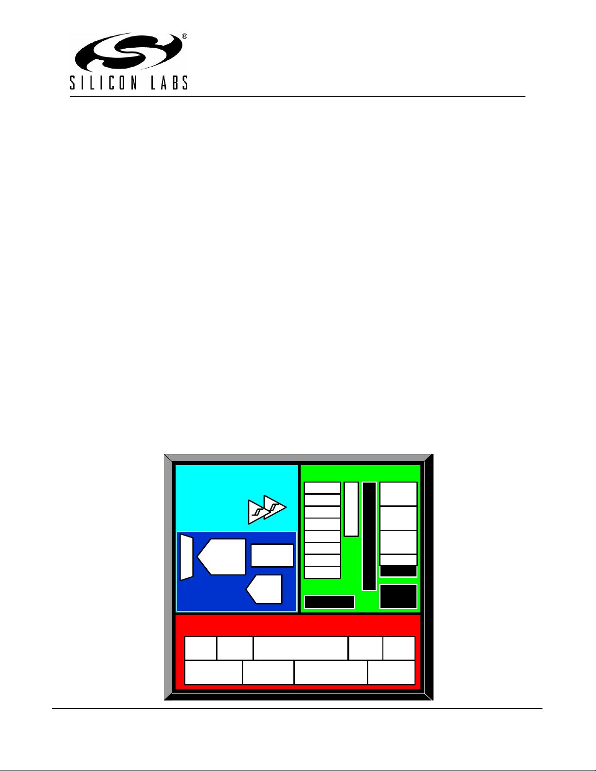
ANALOG
PERIPHERALS
32/16 KB
ISP FLASH
1024 B
SRAM
POR
DEBUG
CIRCUITRY
FLEXIBLE
INTERRUPTS
8051 CPU
(100 or 50 MIPS)
DIGITAL I/O
HIGH-SPEED CONTROLLER CORE
CROSSBAR
WDT
Port 0
Port 1
Port 2
External Memory Interface
Port 4
Port 3
Port 3
48-pin only
16 x 16
MAC
Internal Oscillator /
LFO / PLL
UART
SMBus
PCA
Timer 0
Timer 1
Timer 2
Timer 3
SPI
A
M
U
X
10-bit
200 ksps
ADC
TEMP
SENSOR
10-bit
Current
DAC
‘F360/1/2/6/7/8/9 only
VOLTAGE
COMPARATORS
+
-
+
-


剩余295页未读,继续阅读
资源评论


