没有合适的资源?快使用搜索试试~ 我知道了~
资源推荐
资源详情
资源评论
High Precision, Wideband
RMS-to-DC Converter
AD637
Rev. J
Information furnished by Analog Devices is believed to be accurate and reliable. However, no
responsibility is assumed by Analog Devices for its use, nor for any infringements of patents or other
rights of third parties that may result from its use. Specifications subject to change without notice. No
license is granted by implication or otherwise under any patent or patent rights of Analog Devices.
Trademarks and registered trademarks are the property of their respective owners.
One Technology Way, P.O. Box 9106, Norwood, MA 02062-9106, U.S.A.
Tel: 781.329.4700 www.analog.com
Fax: 781.461.3113 ©2007 Analog Devices, Inc. All rights reserved.
FEATURES
High accuracy
0.02% maximum nonlinearity, 0 V to 2 V rms input
0.10% additional error to crest factor of 3
Wide bandwidth
8 MHz at 2 V rms input
600 kHz at 100 mV rms
Computes
True rms
Square
Mean square
Absolute value
dB output (60 dB range)
Chip select/power-down feature allows
Analog three-state operation
Quiescent current reduction from 2.2 mA to 350 μA
14-lead SBDIP, 14-lead low cost CERDIP, and 16-lead SOIC_W
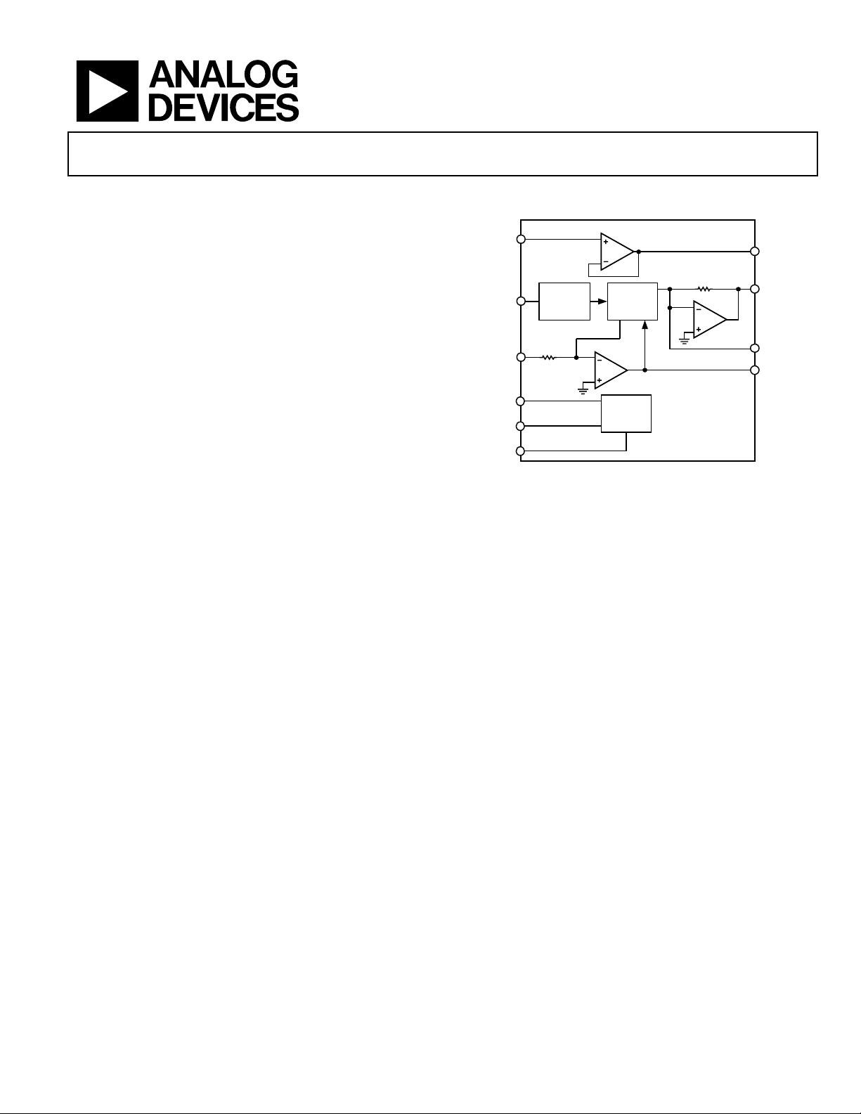
FUNCTIONAL BLOCK DIAGRAM
ABSOLUTE
VALUE
DEN INPUT
RMS OUT
dB OUTPUT
BUFF IN
BUFF
OUT
25kΩ
25kΩ
COMMON
CS
OUTPUT
OFFSET
00788-001
SQUARER/
DIVIDER
BIAS
V
IN
C
AV
AD637
Figure 1.
GENERAL DESCRIPTION
The AD637 is a complete, high accuracy, monolithic rms-to-dc
converter that computes the true rms value of any complex
waveform. It offers performance that is unprecedented in
integrated circuit rms-to-dc converters and comparable to
discrete and modular techniques in accuracy, bandwidth, and
dynamic range. A crest factor compensation scheme in the
AD637 permits measurements of signals with crest factors of
up to 10 with less than 1% additional error. The wide band-
width of the AD637 permits the measurement of signals up to
600 kHz with inputs of 200 mV rms and up to 8 MHz when the
input levels are above 1 V rms.
As with previous monolithic rms converters from Analog
Devices, Inc., the AD637 has an auxiliary dB output available to
users. The logarithm of the rms output signal is brought out to a
separate pin, allowing direct dB measurement with a useful
range of 60 dB. An externally programmed reference current
allows the user to select the 0 dB reference voltage to correspond to
any level between 0.1 V and 2.0 V rms.
A chip select connection on the AD637 permits the user to
decrease the supply current from 2.2 mA to 350 μA during periods
when the rms function is not in use. This feature facilitates the
addition of precision rms measurement to remote or handheld
applications where minimum power consumption is critical. In
addition, when the AD637 is powered down, the output goes to a
high impedance state. This allows several AD637s to be tied
together to form a wideband true rms multiplexer.
The input circuitry of the AD637 is protected from overload
voltages in excess of the supply levels. The inputs are not
damaged by input signals if the supply voltages are lost.
The AD637 is available in accuracy Grade J and Grade K for
commercial temperature range (0°C to 70°C) applications, accuracy
Grade A and Grade B for industrial range (−40°C to +85°C) appli-
cations, and accuracy Grade S rated over the −55°C to +125°C
temperature range. All versions are available in hermetically sealed,
14-lead SBDIP, 14-lead CERDIP, and 16-lead SOIC_W packages.
The AD637 computes the true root mean square, mean square,
or absolute value of any complex ac (or ac plus dc) input
waveform and gives an equivalent dc output voltage. The true
rms value of a waveform is more useful than an average
rectified signal because it relates directly to the power of the
signal. The rms value of a statistical signal is also related to the
standard deviation of the signal.
The AD637 is laser wafer trimmed to achieve rated performance
without external trimming. The only external component
required is a capacitor that sets the averaging time period. The
value of this capacitor also determines low frequency accuracy,
ripple level, and settling time.
The on-chip buffer amplifier can be used either as an input
buffer or in an active filter configuration. The filter can be used
to reduce the amount of ac ripple, thereby increasing accuracy.
AD637
Rev. J | Page 2 of 20
TABLE OF CONTENTS
Features .............................................................................................. 1
Functional Block Diagram .............................................................. 1
General Description ......................................................................... 1
Revision History ............................................................................... 2
Specifications..................................................................................... 3
Absolute Maximum Ratings............................................................ 5
ESD Caution.................................................................................. 5
Pin Configurations and Function Descriptions ........................... 6
Functional Description .................................................................... 7
Standard Connection ................................................................... 8
Chip Select..................................................................................... 8
Optional Trims for High Accuracy............................................ 8
Choosing the Averaging Time Constant....................................9
Frequency Response .................................................................. 11
AC Measurement Accuracy and Crest Factor........................ 12
Connection for dB Output........................................................ 12
dB Calibration............................................................................. 13
Low Frequency Measurements................................................. 14
Vector Summation ..................................................................... 14
Evaluation Board ............................................................................ 16
Outline Dimensions ....................................................................... 19
Ordering Guide .......................................................................... 20
REVISION HISTORY
4/07—Rev. I to Rev. J
Added Evaluation Board Section ................................................. 16
Updated Outline Dimensions....................................................... 20
10/06—Rev. H to Rev. I
Changes to Table 1............................................................................ 3
Changes to Figure 4.......................................................................... 7
Changes to Figure 7.......................................................................... 9
Changes to Figure 16, Figure 18, and Figure 19 ......................... 12
Changes to Figure 20...................................................................... 13
12/05—Rev. G to Rev. H
Updated Format..................................................................Universal
Changes to Figure 1.......................................................................... 1
Changes to Figure 11...................................................................... 10
Updated Outline Dimensions....................................................... 16
Changes to Ordering Guide .......................................................... 17
4/05—Rev. F to Rev. G
Updated Format..................................................................Universal
Changes to Figure 1...........................................................................1
Changes to General Description .....................................................1
Deleted Product Highlights .............................................................1
Moved Figure 4 to Page ....................................................................8
Changes to Figure 5...........................................................................9
Changes to Figure 8........................................................................ 10
Changes to Figure 11, Figure 12, Figure 13, and Figure 14....... 11
Changes to Figure 19...................................................................... 14
Changes to Figure 20...................................................................... 14
Changes to Figure 21...................................................................... 16
Updated Outline Dimensions....................................................... 17
Changes to Ordering Guide.......................................................... 18
3/02—Rev. E to Rev. F
Edits to Ordering Guide ...................................................................3
AD637
Rev. J | Page 3 of 20
SPECIFICATIONS
At 25°C and ±15 V dc, unless otherwise noted.
1
Table 1.
AD637J/AD637A AD637K/AD637B AD637S
Parameter Min Typ Max Min Typ Max Min Typ Max Unit
TRANSFER FUNCTION
V
OUT
=
2
IN
)(V avg × V
OUT
=
2
IN
)(V avg × V
OUT
=
2
IN
)(V avg ×
CONVERSION ACCURACY
Total Error, Internal Trim
2
(
Figure 5)
±1 ± 0.5 ±0.5 ± 0.2 ±1 ± 0.5
mV ±% of
reading
T
MIN
to T
MAX
±3.0 ± 0.6 ±2.0 ± 0.3 ±6 ± 0.7
mV ± % of
reading
vs. Supply
+V
IN
= 300 mV
30
150
30
150
30
150
μV/V
vs. Supply
−V
IN
= −300 mV
100
300
100
300
100
300
μV/V
DC Reversal
Error at 2 V
0.25
0.1
0.25
% of
reading
Nonlinearity 2 V Full Scale
3
0.04
0.02
0.04
% of FSR
Nonlinearity 7 V Full Scale
0.05
0.05
0.05
% of FSR
Total Error, External Trim ±0.5 ± 0.1 ±0.25 ± 0.05 ±0.5 ± 0.1 mV ± % of
reading
ERROR VS. CREST FACTOR
4
Crest Factor 1 to 2 Specified accuracy Specified accuracy Specified accuracy
Crest Factor = 3 ±0.1 ±0.1 ±0.1 % of
reading
Crest Factor = 10 ±1.0 ±1.0 ±1.0 % of
reading
AVERAGING TIME CONSTANT 25 25 25 ms/μF C
AV
INPUT CHARACTERISTICS
Signal Range, ±15 V Supply
Continuous RMS Level 0 to 7 0 to 7 0 to 7 V rms
Peak Transient Input ±15 ±15 ±15 V p-p
Signal Range, ±5 V Supply
Continuous RMS Level 0 to 4 0 to 4 0 to 4 V rms
Peak Transient Input ±6 ±6 ±6 V p-p
Maximum Continuous
Nondestructive
Input Level
(All Supply Voltages)
±15 ±15 ±15 V p-p
Input Resistance 6.4 8 9.6 6.4 8 9.6 6.4 8 9.6 kΩ
Input Offset Voltage ±0.5 ±0.2 ±0.5 mV
FREQUENCY RESPONSE
5
Bandwidth for 1%
Additional Error
(0.09 dB)
V
IN
= 20 mV 11 11 11 kHz
V
IN
= 200 mV 66 66 66 kHz
V
IN
= 2 V 200 200 200 kHz
±3 dB Bandwidth
V
IN
= 20 mV 150 150 150 kHz
V
IN
= 200 mV 1 1 1 MHz
V
IN
= 2 V 8 8 8 MHz
AD637
Rev. J | Page 4 of 20
AD637J/AD637A AD637K/AD637B AD637S
Parameter Min Typ Max Min Typ Max Min Typ Max Unit
OUTPUT CHARACTERISTICS
Offset Voltage
±1
±0.5
±1
mV
vs. Temperature ±0.05
±0.089
±0.04
±0.056
±0.04
±0.07
mV/°C
Voltage Swing,
±15 V Supply, 2 kΩ Load
0 to 12.0
13.5
0 to 12.0
13.5
0 to 12.0
13.5 V
Voltage Swing,
±3 V Supply, 2 kΩ Load
0 to 2
2.2
0 to 2
2.2
0 to 2
2.2 V
Output Current
6
6
6
mA
Short-Circuit Current 20 20 20 mA
Resistance
Chip Select High
0.5 0.5 0.5 Ω
Resistance
Chip Select Low
100 100 100 kΩ
dB OUTPUT
Error, V
IN
7 mV to 7 V rms,
0 dB = 1 V rms
±0.5 ±0.3 ±0.5 dB
Scale Factor −3 −3 −3 mV/dB
Scale Factor Temperature
Coefficient
+0.33 +0.33 +0.33 % of
reading/°C
−0.033 −0.033 −0.033 dB/°C
I
REF
for 0 dB = 1 V rms 5 20
80
5 20
80
5 20
80
μA
I
REF
Range 1 100 1 100 1 100 μA
BUFFER AMPLIFIER
Input Output
Voltage Range
−V
S
to (+V
S
− 2.5 V) −V
S
to (+V
S
− 2.5 V) −V
S
to (+V
S
− 2.5 V) V
Input Offset Voltage ±0.8
±2
±0.5
±1
±0.8
±2
mV
Input Current ±2
±10
±2
±5
±2
±10
nA
Input Resistance 10
8
10
8
10
8
Ω
Output Current −0.13 +5 −0.13 +5 −0.13 +5 mA
Short-Circuit Current 20 20 20 mA
Small Signal Bandwidth 1 1 1 MHz
Slew Rate
6
5 5 5 V/μs
DENOMINATOR INPUT
Input Range 0 to 10 0 to 10 0 to 10 V
Input Resistance 20 25 30 20 25 30 20 25 30 kΩ
Offset Voltage ±0.2 ±0.5 ±0.2 ±0.5 ±0.2 ±0.5 mV
CHIP SELECT (CS)
RMS On Level Open or 2.4 V < V
C
< +V
S
Open or 2.4 V < V
C
< +V
S
Open or 2.4 V < V
C
< +V
S
RMS Off Level V
C
< 0.2 V V
C
< 0.2 V V
C
< 0.2 V
I
OUT
of Chip Select
CS Low 10 10 10 μA
CS High 0 0 0 μA
On Time Constant 10 + ((25 kΩ) × C
AV
) 10 + ((25 kΩ) × C
AV
) 10 + ((25 kΩ) × C
AV
) μs
Off Time Constant 10 + ((25 kΩ) × C
AV
) 10 + ((25 kΩ) × C
AV
) 10 + ((25 kΩ) × C
AV
) μs
POWER SUPPLY
Operating Voltage Range
±3.0
±18 ±3.0
±18 ±3.0
±18
V
Quiescent Current 2.2
3
2.2
3
2.2
3
mA
Standby Current 350
450
350
450
350
450
μA
1
Specifications shown in bold are tested on all production units at final electrical test. Results from those tests are used to calculate outgoing quality levels.
All minimum and maximum specifications are guaranteed, although only those shown in boldface are tested on all production units.
2
Accuracy specified 0 V rms to 7 V rms dc with AD637 connected, as shown in Figure 5.
3
Nonlinearity is defined as the maximum deviation from the straight line connecting the readings at 10 mV and 2 V.
4
Error vs. crest factor is specified as additional error for 1 V rms.
5
Input voltages are expressed in volts rms. Percent is in % of reading.
6
With external 2 kΩ pull-down resistor tied to −V
S
.
剩余19页未读,继续阅读
资源评论
学工科的皮皮志^_^
- 粉丝: 2w+
- 资源: 7
上传资源 快速赚钱
- 我的内容管理 展开
- 我的资源 快来上传第一个资源
- 我的收益 登录查看自己的收益
- 我的积分 登录查看自己的积分
- 我的C币 登录后查看C币余额
- 我的收藏
- 我的下载
- 下载帮助
安全验证
文档复制为VIP权益,开通VIP直接复制
信息提交成功