


Space Vector Control of a
Three Phase Rectifier using PLECS
Dr. John Schönberger
Plexim GmbH, Zürich
1 Introduction
Space vector control is popular for controlling mo-
tor drives or three-phase rectifiers since it offers
reduced switching losses and better utilization of
the dc bus compared to conventional PWM modula-
tion. This report describes a space vector controller
for a three-phase boost-type rectifier that is imple-
mented in PLECS. The schematic diagram of the
boost rectifier is shown in Fig. 1. The source is a 50
Hz supply and the load is a constant current source
that behaves like an infinite inductor.
2 Space Vector Control
The control goal for the three-phase boost rectifier is
to generate sinusoidal input currents and regulate
the dc output voltage. Current control is achieved
using an inner current control loop that measures
the phase current, I
n
, and controls the inductor-
neutral voltage, v
n1
, to force the phase current to
track its reference value. The current reference is
provided by outer control loops that implement dc
voltage and power factor control.
With space vector control, the inductor-neutral
voltage is controlled as a vector quantity in the αβ
or dq domain. In this example, control is performed
in the dq domain. The advantage of dq control is
that ac quantities become dc quantities in the dq
domain. Thus no tracking error exists when using
a PI controller to regulate the ac input current.
Figure 1: Three-phase rectifier schematic diagram.
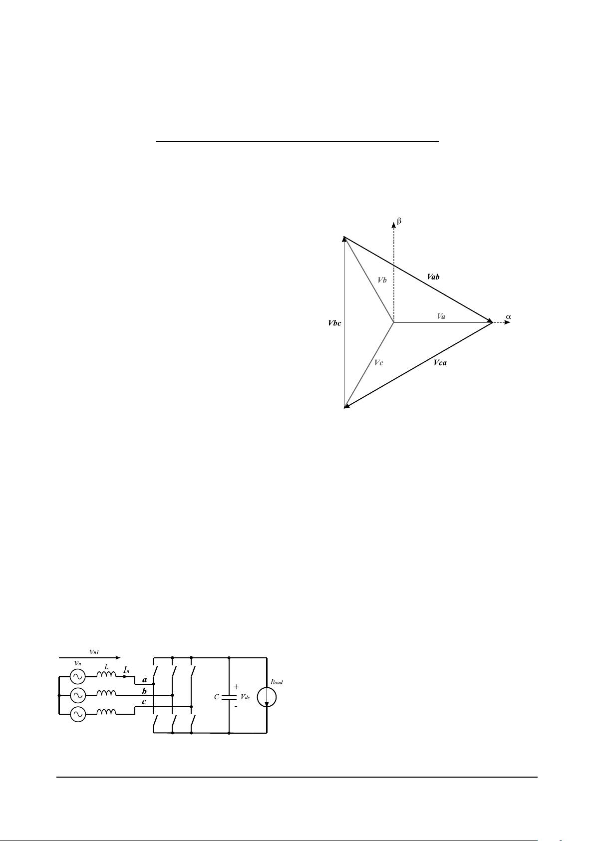
Figure 2: Line voltage vectors in αβ domain.
2.1 Switching States
For the three-phase rectifier, the ac-side voltage re-
quired to induce sinusoidal currents through the in-
ductors is first calculated. This reference vector,
v
n1
, is generated by time-averaging the available
switching vectors. A switching vector is created
on the ac-side of the rectifier by applying certain
switch combinations to the rectifier bridge.
The line voltage vectors that are shown in Fig. 2
as vectors in the αβ plane are added or subtracted
to obtain the switching vector for a unique switch-
ing combination. Because the input lines can not
be shorted and continuous current must be main-
tained at the output, the switching states are re-
stricted to eight combinations. Fig. 3 shows the two
example switching states, (100) and (110), that are
applied to the rectifier bridge. With switching state
(100), V
ab
= V
dc
, V
bc
=0and V
ca
= −V
dc
. The resul-
tant switching vector for this state can be derived
by summing these line voltage vectors. The graphi-
cal derivation of switching vectors (100) and (110) is
shown in Fig. 4. The complete set of switching vec-
tors in the αβ plane is shown in Fig. 5 along with
the sectors encompassed by each pair of switching
vectors. The vectors (000) and (111) are both zero
version 02-11


