


DS-25SF081–045I–8/2017
Features
Single 2.3V - 3.6V Supply
Serial Peripheral Interface (SPI) Compatible
Supports SPI Modes 0 and 3
Supports Dual and Quad Output Read
104MHz Maximum Operating Frequency
Clock-to-Output (t
V
) of 6 ns
Flexible, Optimized Erase Architecture for Code + Data Storage Applications
Uniform 4-Kbyte Block Erase
Uniform 32-Kbyte Block Erase
Uniform 64-Kbyte Block Erase
Full Chip Erase
Hardware Controlled Locking of Protected Blocks via WP Pin
3 Protected Programmable Security Register Pages
Flexible Programming
Byte/Page Program (1 to 256 Bytes)
Fast Program and Erase Times
0.7ms Typical Page Program (256 Bytes) Time
70ms Typical 4-Kbyte Block Erase Time
300ms Typical 32-Kbyte Block Erase Time
600ms Typical 64-Kbyte Block Erase Time
JEDEC Standard Manufacturer and Device ID Read Methodology
Low Power Dissipation
2µA Deep Power-Down Current (Typical)
10µA Standby current (Typical)
4mA Active Read Current (Typical)
Endurance: 100,000 Program/Erase Cycles
Data Retention: 20 Years
Complies with Full Industrial Temperature Range
Industry Standard Green (Pb/Halide-free/RoHS Compliant) Package Options
8-lead SOIC (150-mil and 208-mil)
8-pad Ultra Thin DFN (5 x 6 x 0.6 mm and 2 x 3 x 0.6 mm)
8-lead TSSOP (4 x 4 mm)
Die in Wafer Form
AT25SF081
8-Mbit, 2.3V Minimum
SPI Serial Flash Memory with Dual-I/O and Quad-IO Support
8Mbit -> 1Mkb

2
AT25SF081
DS-25SF081–045I–8/2017
Description
The Adesto
®
AT25SF081 is a serial interface Flash memory device designed for use in a wide variety of high-volume
consumer based applications in which program code is shadowed from Flash memory into embedded or external RAM
for execution. The flexible erase architecture of the AT25SF081 is ideal for data storage as well, eliminating the need for
additional data storage devices.
The erase block sizes of the AT25SF081 have been optimized to meet the needs of today's code and data storage
applications. By optimizing the size of the erase blocks, the memory space can be used much more efficiently. Because
certain code modules and data storage segments must reside by themselves in their own erase regions, the wasted and
unused memory space that occurs with large block erase Flash memory devices can be greatly reduced. This increased
memory space efficiency allows additional
code routines and data storage segments to be added while still maintaining
the same overall device density.
The device also contains three pages of Security Register that can be used for purposes such as unique device
serialization, system-level Electronic Serial Number (ESN) storage, locked key storage, etc. These Security Register
pages can be individually locked.
1. Pin Descriptions and Pinouts
Table 1-1. Pin Descriptions
Symbol Name and Function
Asserted
State
Type
CS
CHIP SELECT: Asserting the CS pin selects the device. When the CS pin is deasserted, the
device will be deselected and normally be placed in standby mode (not Deep Power-Down
mode), and the SO pin will be in a high-impedance state. When the device is deselected,
data will not be accepted on the SI pin.
A high-to-low transition on the CS
pin is required to start an operation, and a low-to-high
transition is required to end an operation. When ending an internally self-timed operation
such as a program or erase cycle, the device will not enter the standby mode until the
completion of the operation.
Low Input
SCK
SERIAL CLOCK: This pin is used to provide a clock to the device and is used to control the
flow of data to and from the device. Command, address, and input data present on the SI pin
is always latched in on the rising edge of SCK, while output data on the SO pin is always
clocked out on the falling edge of SCK.
- Input
SI (I/O
0
)
SERIAL INPUT: The SI pin is used to shift data into the device. The SI pin is used for all data
input including command and address sequences. Data on the SI pin is always latched in on
the rising edge of SCK.
With the Dual-Output and Quad-Output Read commands, the SI Pin becomes an output pin
(I/O
0
) in conjunction with other pins to allow two or four bits of data on (I/O
3-0
) to be clocked
in on every falling edge of SCK
To maintain consistency with the SPI nomenclature, the SI (I/O
0
) pin will be referenced as
the SI pin unless specifically addressing the Dual-I/O and Quad-I/O modes in which case it
will be referenced as I/O
0
Data present on the SI pin will be ignored whenever the device is deselected (CS is
deasserted).
- Input/Output

3
AT25SF081
DS-25SF081–045I–8/2017
SO (I/O
1
)
SERIAL OUTPUT: The SO pin is used to shift data out from the device. Data on the SO pin
is always clocked out on the falling edge of SCK.
With the Dual-Output Read commands, the SO Pin remains an output pin (I/O
0
) in
conjunction with other pins to allow two bits of data on (I/O
1-0
) to be clocked in on every
falling edge of SCK
To maintain consistency with the SPI nomenclature, the SO (I/O
1
) pin will be referenced as
the SO pin unless specifically addressing the Dual-I/O modes in which case it will be
referenced as I/O
1
The SO pin will be in a high-impedance state whenever the device is deselected (CS is
deasserted).
- Input/Output
WP
(I/O
2
)
WRITE PROTECT: The WP pin controls the hardware locking feature of the device. With the
Quad-Output Read commands, the WP Pin becomes an output pin (I/O
2
) in conjunction with
other pins to allow four bits of data on (I/O3
3-0
) to be clocked in on every falling edge of SCK.
To maintain consistency with the SPI nomenclature, the WP
(I/O
2
) pin will be referenced as
the WP pin unless specifically addressing the Quad-I/O modes in which case it will be
referenced as I/O
2
The WP pin is internally pulled-high and may be left floating if hardware controlled protection
will not be used. However, it is recommended that the WP
pin also be externally connected
to V
CC
whenever possible.
- Input/Output
HOLD
(I/O
3
)
HOLD: The HOLD pin is used to temporarily pause serial communication without
deselecting or resetting the device. While the HOLD pin is asserted, transitions on the SCK
pin and data on the SI pin will be ignored, and the SO pin will be in a high-impedance state.
The CS
pin must be asserted, and the SCK pin must be in the low state in order for a Hold
condition to start. A Hold condition pauses serial communication only and does not have an
effect on internally self-timed operations such as a program or erase cycle. Please refer to
“Hold Function” on page 31 for additional details on the Hold operation.
With the Quad-Output Read commands, the HOLD
Pin becomes an output pin (I/O
3
) in
conjunction with other pins to allow four bits of data on (I/O3
3-0
) to be clocked in on every
falling edge of SCK.
To maintain consistency with the SPI nomenclature, the HOLD
(I/O
3
) pin will be referenced
as the HOLD pin unless specifically addressing the Quad-I/O modes in which case it will be
referenced as I/O
3
The HOLD pin is internally pulled-high and may be left floating if the Hold function will not be
used. However, it is recommended that the HOLD pin also be externally connected to V
CC
whenever possible.
- Input/Output
V
CC
DEVICE POWER SUPPLY: The V
CC
pin is used to supply the source voltage to the device.
Operations at invalid V
CC
voltages may produce spurious results and should not be
attempted.
- Power
GND
GROUND: The ground reference for the power supply. GND should be connected to the
system ground.
- Power
Table 1-1. Pin Descriptions (Continued)
Symbol Name and Function
Asserted
State Type

4
AT25SF081
DS-25SF081–045I–8/2017
2. Block Diagram
Figure 2-1. Block Diagram
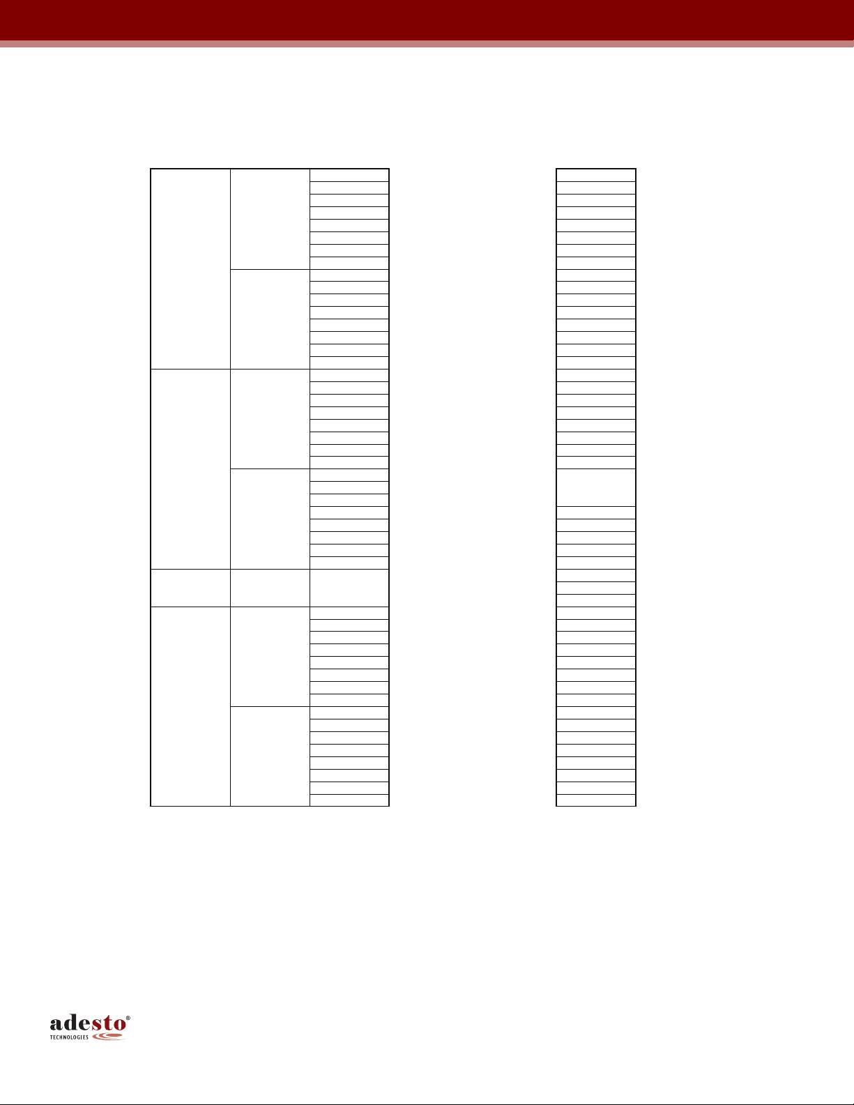
3. Memory Array
To provide the greatest flexibility, the memory array of the AT25SF081 can be erased in four levels of granularity
including a full chip erase. The size of the erase blocks is optimized for both code and data storage applications, allowing
both code and data segments to reside in their own erase regions. The Memory Architecture Diagram illustrates the
breakdown of each erase level.
Figure 1-1. 8-SOIC, 8-TSSOP (Top View) Figure 1-2. 8-UDFN (Top View)
1
2
3
4
8
7
6
5
CS
SO
WP
GND
VCC
HOLD
SCK
SI
CS
SO
WP
GND
1
2
3
4
8
7
6
5
VCC
HOLD
SCK
SI
Flash
Memory
Array
Y-Gating
CS
SCK
Note: I/O
3-0
pin naming convention is used for Dual-I/O and Quad-I/O commands.
SO (I/O
1
)
SI (I/O
0
)
Y-Decoder
Address Latch
X-Decoder
I/O Buffers
and Latches
Control and
Protection Logic
SRAM
Data Buffer
WP (I/O
2
)
Interface
Control
And
Logic
HOLD (I/O
3
)
5
AT25SF081
DS-25SF081–045I–8/2017
Figure 3-1. Memory Architecture Diagram
64KB 32KB 4KB 1-256 Byte
4KB
0FFFFFh–0FF000h 256 Bytes 0FFFFFh–0FFF00h
4KB
0FEFFFh–0FE000h 256 Bytes 0FFEFFh–0FFE00h
4KB
0FDFFFh–0FD000h 256 Bytes 0FFDFFh–0FFD00h
4KB
0FCFFFh–0FC000h 256 Bytes 0FFCFFh–0FFC00h
4KB
0FBFFFh–0FB000h 256 Bytes 0FFBFFh–0FFB00h
4KB
0FAFFFh–0FA000h 256 Bytes 0FFAFFh–0FFA00h
4KB
0F9FFFh–0F9000h 256 Bytes 0FF9FFh–0FF900h
4KB
0F8FFFh–0F8000h 256 Bytes 0FF8FFh–0FF800h
4KB
0F7FFFh–0F7000h 256 Bytes 0FF7FFh–0FF700h
4KB
0F6FFFh–0F6000h 256 Bytes 0FF6FFh–0FF600h
4KB
0F5FFFh–0F5000h 256 Bytes 0FF5FFh–0FF500h
4KB
0F4FFFh–0F4000h 256 Bytes 0FF4FFh–0FF400h
4KB
0F3FFFh–0F3000h 256 Bytes 0FF3FFh–0FF300h
4KB
0F2FFFh–0F2000h 256 Bytes 0FF2FFh–0FF200h
4KB
0F1FFFh–0F1000h 256 Bytes 0FF1FFh–0FF100h
4KB
0F0FFFh–0F0000h 256 Bytes 0FF0FFh–0FF000h
4KB
0EFFFFh–0EF000h 256 Bytes 0FEFFFh–0FEF00h
4KB
0EEFFFh–0EE000h 256 Bytes 0FEEFFh–0FEE00h
4KB
0EDFFFh–0ED000h 256 Bytes 0FEDFFh–0FED00h
4KB
0ECFFFh–0EC000h 256 Bytes 0FECFFh–0FEC00h
4KB
0EBFFFh–0EB000h 256 Bytes 0FEBFFh–0FEB00h
4KB
0EAFFFh–0EA000h 256 Bytes 0FEAFFh–0FEA00h
4KB
0E9FFFh–0E9000h 256 Bytes 0FE9FFh–0FE900h
4KB
0E8FFFh–0E8000h 256 Bytes 0FE8FFh–0FE800h
4KB
0E7FFF
h–0E7000h
4KB
0E6FFF
h–0E6000h
4KB
0E5FFF
h–0E5000h
4KB
0E4FFFh–0E4000h 256 Bytes 0017FFh–001700h
4KB
0E3FFFh–0E3000h 256 Bytes 0016FFh–001600h
4KB
0E2FFFh–0E2000h 256 Bytes 0015FFh–001500h
4KB
0E1FFFh–0E1000h 256 Bytes 0014FFh–001400h
4KB
0E0FFFh–0E0000h 256 Bytes 0013FFh–001300h
256 Bytes 0012FFh–001200h
256 Bytes 0011FFh–001100h
256 Bytes 0010FFh–001000h
4KB
00FFFFh–00F000h 256 Bytes 000FFFh–000F00h
4KB
00EFFFh–00E000h 256 Bytes 000EFFh–000E00h
4KB
00DFFFh–00D000h 256 Bytes 000DFFh–000D00h
4KB
00CFFFh–00C000h 256 Bytes 000CFFh–000C00h
4KB
00BFFFh–00B000h 256 Bytes 000BFFh–000B00h
4KB
00AFFFh–00A000h 256 Bytes 000AFFh–000A00h
4KB
009FFFh–009000h 256 Bytes 0009FFh–000900h
4KB
008FFFh–008000h 256 Bytes 0008FFh–000800h
4KB
007FFFh–007000h 256 Bytes 0007FFh–000700h
4KB
006FFFh–006000h 256 Bytes 0006FFh–000600h
4KB
005FFFh–005000h 256 Bytes 0005FFh–000500h
4KB
004FFFh–004000h 256 Bytes 0004FFh–000400h
4KB
003FFFh–003000h 256 Bytes 0003FFh–000300h
4KB
002FFFh–002000h 256 Bytes 0002FFh–000200h
4KB
001FFFh–001000h 256 Bytes 0001FFh–000100h
4KB
000FFFh–000000h 256 Bytes 0000FFh–000000h
• • •
64KB
Sector 0
Block Erase Detail Page Program Detail
Page AddressBlock Address
32KB
32KB
Range
•
• •
• • •
Range
32KB
32KB
• •
•
64KB
Sector 15
32KB
32KB
64KB
Sector 14
4种擦除方式,4、32、
64、full


评论0
最新资源