32Meg x 8, 16Meg x16 256Mb SYNCHRONOUS DRAM手册
需积分: 0 137 浏览量
2024-05-12
20:41:04
上传
评论
收藏 863KB PDF 举报

IS42S83200G, IS42S16160G
IS45S83200G, IS45S16160G
Integrated Silicon Solution, Inc. — www.issi.com 1
Rev. A
3/20/2012
Copyright © 2012 Integrated Silicon Solution, Inc. All rights reserved. ISSI reserves the right to make changes to this specification and its products at any time with-
out notice. ISSI assumes no liability arising out of the application or use of any information, products or services described herein. Customers are advised to obtain
the latest version of this device specification before relying on any published information and before placing orders for products.
Integrated Silicon Solution, Inc. does not recommend the use of any of its products in life support applications where the failure or malfunction of the product can
reasonably be expected to cause failure of the life support system or to significantly affect its safety or effectiveness. Products are not authorized for use in such ap-
plications unless Integrated Silicon Solution, Inc. receives written assurance to its satisfaction, that:
a.) the risk of injury or damage has been minimized;
b.) the user assume all such risks; and
c.) potential liability of Integrated Silicon Solution, Inc is adequately protected under the circumstances
FEATURES
• Clock frequency: 166, 143 MHz
• Fully synchronous; all signals referenced to a
positive clock edge
• Internal bank for hiding row access/precharge
• Single Power supply: 3.3V + 0.3V
• LVTTL interface
• Programmable burst length
– (1, 2, 4, 8, full page)
• Programmable burst sequence:
Sequential/Interleave
• Auto Refresh (CBR)
• Self Refresh
• 8K refresh cycles every 32 ms (A2 grade) or
64 ms (commercial, industrial, A1 grade)
• Random column address every clock cycle
• Programmable CAS latency (2, 3 clocks)
• Burst read/write and burst read/single write
operations capability
• Burst termination by burst stop and precharge
command
OPTIONS
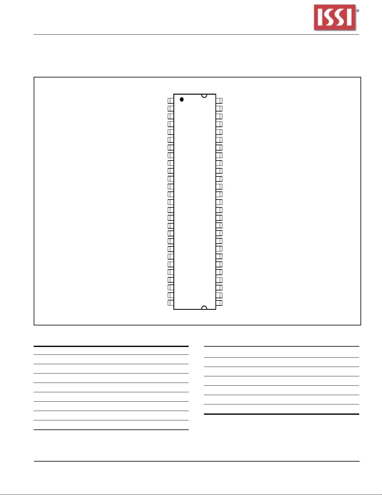
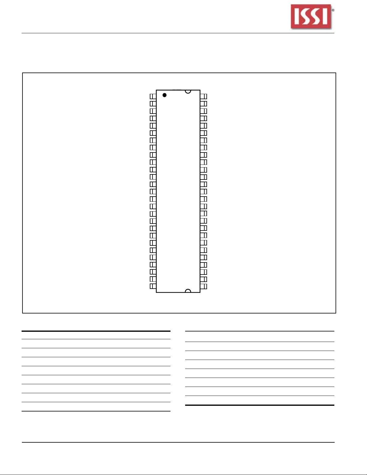
• Package:
54-pin TSOP-II
54-ball BGA
• Operating Temperature Range:
Commercial (0
o
C to +70
o
C)
Industrial (-40
o
C to +85
o
C)
Automotive Grade A1 (-40
o
C to +85
o
C)
Automotive Grade A2 (-40
o
C to +105
o
C)
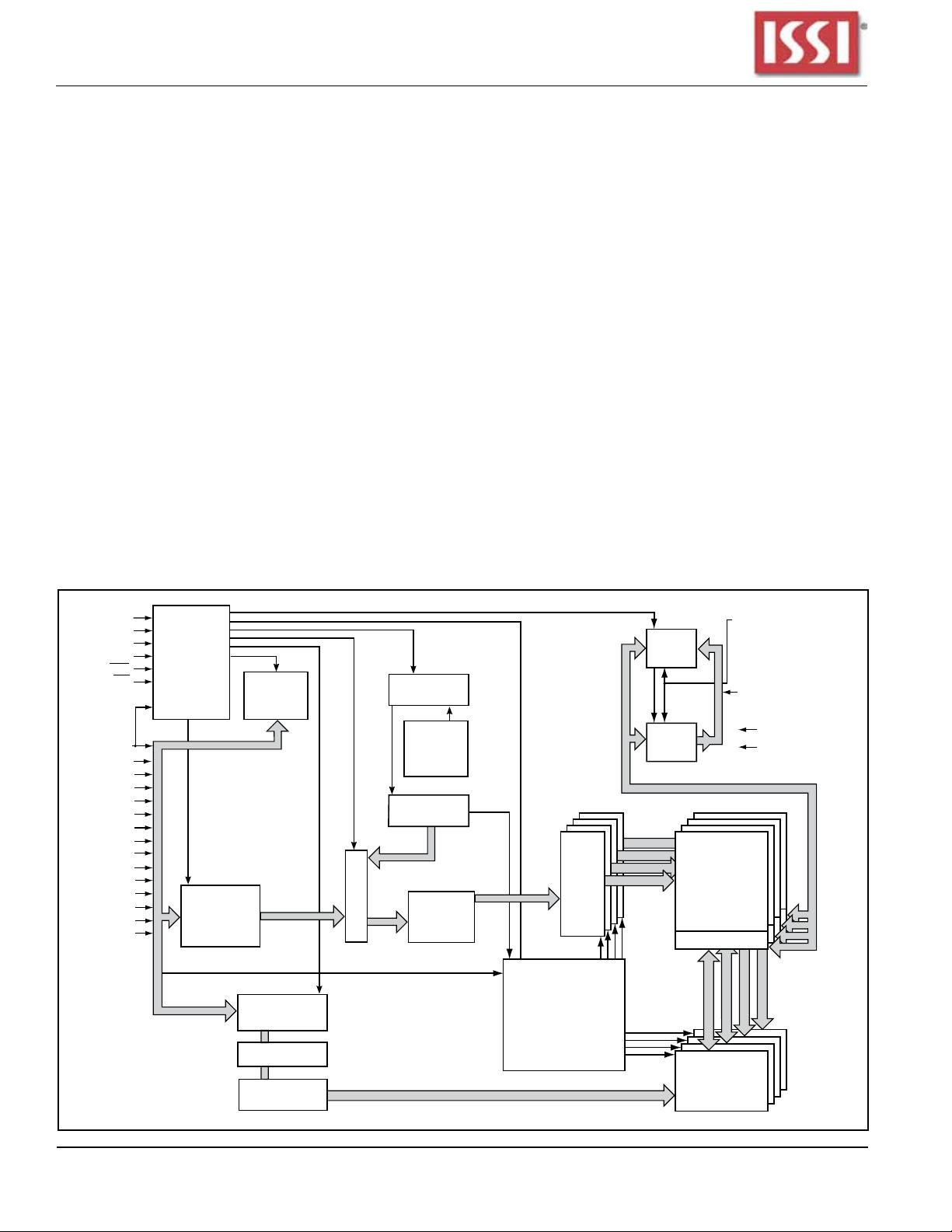
OVERVIEW
ISSI's 256Mb Synchronous DRAM achieves high-speed
data transfer using pipeline architecture. All inputs and
outputs signals refer to the rising edge of the clock input.
The 256Mb SDRAM is organized as follows.
32Meg x 8, 16Meg x16
256Mb SYNCHRONOUS DRAM
MARCH 2012
IS42S83200G IS42S16160G
8M x 8 x 4 Banks 4M x16x4 Banks
54-pin TSOPII 54-pin TSOPII
54-ball BGA 54-ball BGA
Parameter 32M x 8 16M x 16
Conguration 8M x 8 x 4
banks
4M x 16 x 4
banks
Refresh Count
Com./Ind.
A1
A2
8K/64ms
8K/64ms
8K/16ms
8K/64ms
8K/64ms
8K/16ms
Row Addresses A0-A12 A0-A12
Column Addresses A0-A9 A0-A8
Bank Address Pins BA0, BA1 BA0, BA1
Auto Precharge Pins A10/AP A10/AP
ADDRESS TABLE
KEY TIMING PARAMETERS
Parameter -6 -7 Unit
Clk Cycle Time
CAS Latency = 3 6 7 ns
CAS Latency = 2 10 7.5 ns
Clk Frequency
CAS Latency = 3 166 143 Mhz
CAS Latency = 2 100 133 Mhz
Access Time from Clock
CAS Latency = 3 5.4 5.4 ns
CAS Latency = 2 6.5 5.4 ns
剩余62页未读,继续阅读
资源评论


伊宇韵
- 粉丝: 2056
- 资源: 3


最新资源
- 01-spring-boot-overview
- vgg模型-基于深度学习AI算法对猫的动作行为识别-不含数据集图片-含逐行注释和说明文档.zip
- vgg模型-CNN图像分类识别人脸-不含数据集图片-含逐行注释和说明文档.zip
- Detect It Easy v3.03
- shufflenet模型-基于人工智能的卷积网络训练识别鞋类-不含数据集图片-含逐行注释和说明文档.zip
- shufflenet模型-python语言pytorch框架训练识别樱桃新鲜度-不含数据集图片-含逐行注释和说明文档.zip
- 优质资源,让 .NET 开发更简单,更通用,更流行
- resnet模型-基于深度学习对苹果颜色识别-不含数据集图片-含逐行注释和说明文档.zip
- mobilenet模型-基于图像分类算法对食物美食识别-不含数据集图片-含逐行注释和说明文档.zip
- ImmunityDebugger
资源上传下载、课程学习等过程中有任何疑问或建议,欢迎提出宝贵意见哦~我们会及时处理!
点击此处反馈


