没有合适的资源?快使用搜索试试~ 我知道了~
MPS同步降压芯片MP9928 中文手册
1星 需积分: 32 5 下载量 158 浏览量
2022-10-22
19:41:13
上传
评论
收藏 897KB PDF 举报
温馨提示
试读
25页
MPS同步降压芯片MP9928 中文手册
资源详情
资源评论
资源推荐
MP9928
4V-60V Input, Current Mode,
Synchronous Step-Down
Controller
同步降压
MP9928 Rev. 1.1 www.MonolithicPower.com 1
8/24/2018 MPS Proprietary Information. Patent Protected. Unauthorized Photocopy and Duplication Prohibited.
© 2018 MPS. All Rights Reserved.
The Future of Analog
模拟
IC Technology
DESCRIPTION
The MP9928 is a high-voltage, synchronous
step-down switching regulator
调整
controller
that
can directly step down voltages from up to
60V.
The MP9928 uses PWM current
control
architecture with accurate
cycle-by-cycle
current limiting.
精确逐周期限流的架构
It is capable of driving
dual N-
channel MOSFET switches.
AAM Mode (Advanced asynchronous
mode
高级异步模式
)
enables non-synchronous
operation and PFM
mode to optimize light load
efficiency.
支持异步操作和PFM模式,以优化轻负
载效率。
The operating frequency of MP9928 can be
programmed by an external resistor or
synchronized to an external clock for noise-
sensitive applications. Fault protections are
available including a precision output over
voltage protection (OVP), output over current
protection (OCP), and thermal shutdown.
The MP9928 is available in TSSOP20-EP
package and QFN-20 (3mmx4mm) package.
FEATURES
Wide 4V to 60V Operating Input Range
Dual N-Channel MOSFET Driver
Low Dropout Operation: Maximum Duty
Cycle at 99.5%
Programmable Frequency Range: 100kHz -
1000kHz
180º Out-of-Phase SYNCO
External Soft-Start and PG Pin
Selectable Cycle-by-Cycle Current Limit
Output Over Voltage Protection
Internal LDO with Externally Power Supply
Option
Programmable CCM and AAM Pulse-
Skipping Mode
Accuracy
精确
Over Temperature Protection
TSSOP20-EP package and QFN-20
(3mmx4mm) Package
APPLICATIONS
PD Power Supply in PoE System
USB Dedicated Charging Port (DCP)
Industrial Control Systems
Power Supply for Linear Chargers
All MPS parts are lead-free, halogen-free, and adhere to the RoHS
directive. For MPS green status, please visit the MPS website under quality
assurance. “MPS” and “The Future of Analog IC Technology” are
registered trademarks of Monolithic Power Systems, Inc.
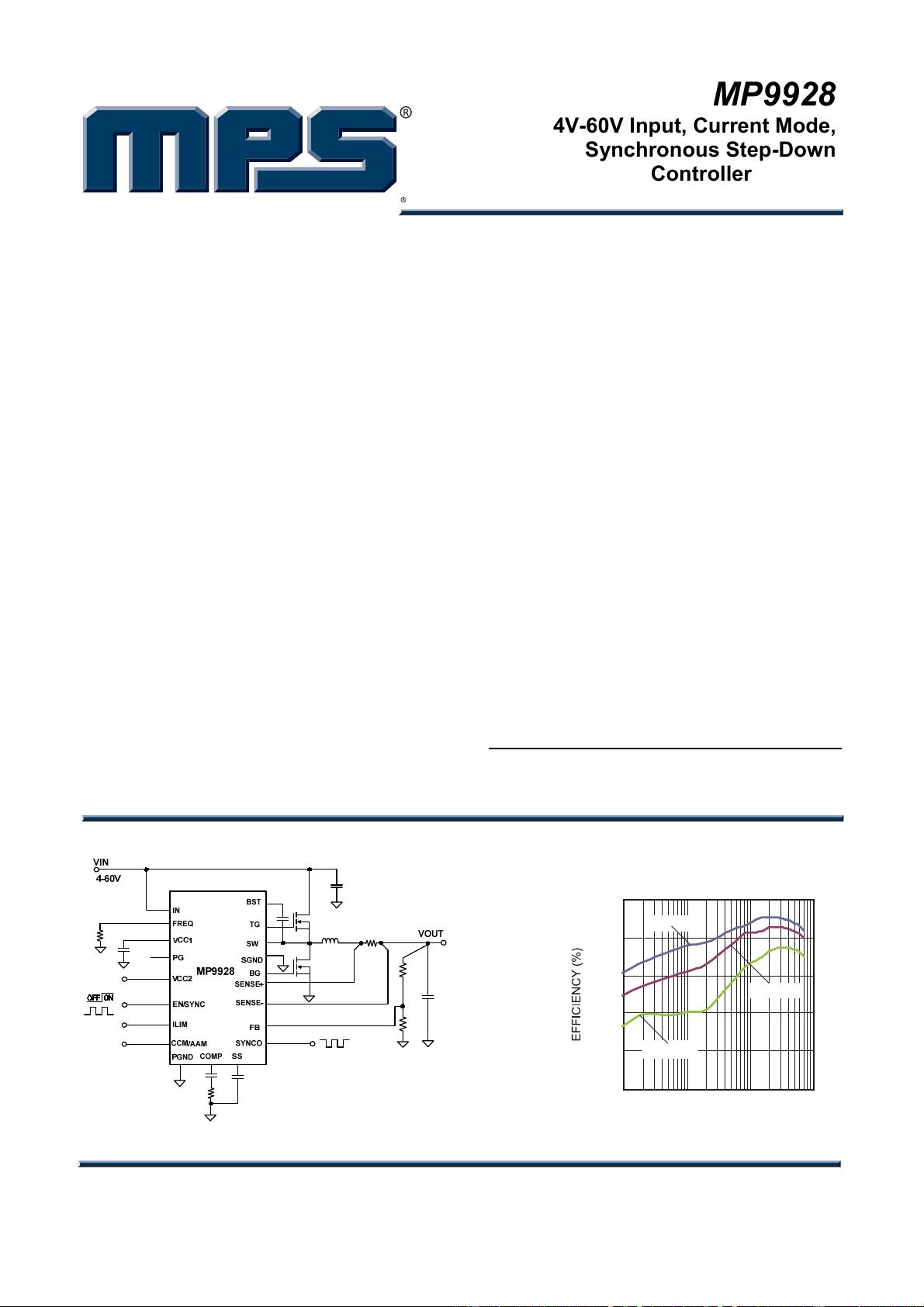
TYPICAL APPLICATION
OUTPUT CURRENT(A)
Efficiency
V
OUT
=5V, AAM
50
60
70
80
90
100
0.01 0.1 1 10
V
IN
=12V
V
IN
=24V
V
IN
=48V
MP9928—4V TO 60V SYNCHRONOUS STEP-DOWN CONTROLLER
MP9928 Rev. 1.1 www.MonolithicPower.com 2
8/24/2018 MPS Proprietary Information. Patent Protected. Unauthorized Photocopy and Duplication Prohibited.
© 2018 MPS. All Rights Reserved.
ORDERING INFORMATION
Part Number Package Top Marking
MP9928GF* TSSOP-20 EP See Below
MP9928GL** QFN-20 (3mmx4mm) See Below
* For Tape & Reel, add suffix –Z (e.g. MP9928GF–Z)
** For Tape & Reel, add suffix –Z (e.g. MP9928GL–Z)
TOP MARKING (MP9928GF)
MP9928: product code of MP9928GF;
MPS: MPS prefix;
YY: year code;
WW: week code:
LLLLLLLLL: lot number;
TOP MARKING (MP9928GL)
9928: product code of MP9928GL;
MP: MPS prefix;
Y: year code;
W: week code:
LLL: lot number;
MP9928—4V TO 60V SYNCHRONOUS STEP-DOWN CONTROLLER
MP9928 Rev. 1.1 www.MonolithicPower.com 3
8/24/2018 MPS Proprietary Information. Patent Protected. Unauthorized Photocopy and Duplication Prohibited.
© 2018 MPS. All Rights Reserved.
PACKAGE REFERENCE
TOP VIEW TOP VIEW
TSSOP-20 EP QFN-20 (3mmx4mm)
ABSOLUTE MAXIMUM RATINGS
(1)
Input supply voltage (V
IN
) ................ -0.3V to 65V
EN/SYNC ........................................ -0.3V to 50V
SW ........................... -0.3V(-4V for <20ns) to 65V
BST - SW ....................................... -0.3V to 6.5V
Supply voltage (VCC1) .................. -0.3V to 6.5V
External supply voltage (VCC2) ..... -0.3V to 15V
SENSE + / - ..................................... -0.3V to 28V
Differential sense (SENSE+ to SENSE-) ............
...................................................... -0.7V to +0.7V
TG ............................... V
SW
- 0.3V to V
BST
+ 0.3V
BG .................................... -0.3V to VCC1 + 0.3V
All other pins ................................ -0.3V to +6.5V
Continuous power dissipation (T
A
= +25°C)
(2)
TSSOP-20 EP ............................................. 3.1W
QFN-20 (3mmx4mm) .................................. 2.6W
Junction temperature ............................... .150C
Lead temperature ...................................... 260C
Storage temperature ................. -65C to +175C
Recommended Operating Conditions
(3)
Supply voltage (V
IN
) .......................... 4V to 60V
(4)
Output voltage (V
OUT
) .................................. ≤24V
Supply voltage for (VCC2) .................. 5V to 12V
Operating junction temp. (T
J
). ... -40°C to +125°C
Thermal Resistance
(5)
θ
JA
θ
JC
TSSOP-20 EP ......................... 40 ........ 8 .... C/W
QFN-20 (3mmx4mm) .............. 48 ....... 10 ... C/W
NOTES:
1) Exceeding these ratings may damage the device.
2) The maximum allowable power dissipation is a function of the
maximum junction temperature T
J
(MAX), the junction-to-
ambient thermal resistance θ
JA
, and the ambient temperature
T
A
. The maximum allowable continuous power dissipation at
any ambient temperature is calculated by P
D
(MAX) = (T
J
(MAX)-T
A
)/θ
JA
. Exceeding the maximum allowable powe
r
dissipation produces an excessive die temperature, causing
the regulator to go into thermal shutdown. Internal thermal
shutdown circuitry protects the device from permanent
damage.
3) The device is not guaranteed to function outside of its
operating conditions.
4) UVLO_rising is 5V but UVLO_falling is lower than 4V, so
input must be >5V for startup, and after start up MP9928 can
work down to 4V input voltage.
5) Measured on JESD51-7, 4-layer PCB.
MP9928—4V TO 60V SYNCHRONOUS STEP-DOWN CONTROLLER
MP9928 Rev. 1.1 www.MonolithicPower.com 4
8/24/2018 MPS Proprietary Information. Patent Protected. Unauthorized Photocopy and Duplication Prohibited.
© 2018 MPS. All Rights Reserved.
ELECTRICAL CHARACTERISTICS
V
IN
= 24V, T
J
= -40C to 125C, EN = 2V, V
ILIMIT
= 75mV, unless otherwise noted.
Parameters Symbol Condition Min Typ Max Units
Input Supply
V
IN
UVLO threshold (rising)
IN
UV
_
RISING
4.5 5 V
V
IN
UVLO threshold (falling)
IN
UV
_
FALLING
3.7 3.95 V
V
IN
UVLO hysteresis IN
UV
_
HYS
800 mV
V
IN
supply current with VCC2 bias I
Q
_
VCC2
VCC2 = 12V, external bias 25 40 μA
V
IN
supply current without VCC2
bias
I
Q
VCC2 = 0, V
FB
= 0.84V, V
AAM
= 5V,
SENSE+ = SENSE- = 0.3V
750 1000 μA
V
IN
AAM current I
Q
_
AAM
V
AAM
=0.6V, V
FB
=0.84V,
SENSE+ = SENSE- = 0.3V
250 350 μA
V
IN
shutdown current I
SHDN
V
EN
= 0V 0.5 3 μA
V
CC
Regulator
VCC1 regulator output voltage
from V
IN
VCC1_
VIN
VIN > 6V 5 V
VCC1 regulator load regulation
from V
IN
Load = 0 to 50mA,
VCC2
floating or connects to GND
1 3 %
VCC1 regulator output voltage
from VCC2
VCC1_
VCC2
VCC2 > 6V 5 V
VCC1 regulator load regulation
from VCC2
Load = 0 to 50mA, VCC2 = 12V 1 3 %
VCC2 UVLO threshold (rising)
VCC2_
RISING
4.7 4.92 V
VCC2 UVLO threshold (falling)
VCC2_
FALLING
4.45 V
VCC2 threshold hysteresis VCC2_
HYS
250 mV
VCC2 supply current I
VCC2
V
AAM
= 5V, V
FB
= 0.84V,
VCC2 = 12V
800 1200 μA
V
AAM
= 0.6V,
V
FB
= 0.84V, VCC2 = 12V
200 300 μA
Feedback (FB)
Feedback voltage
V
FB
4V V
IN
60V, T
J
=25C
0.792 0.800 0.808 V
4V V
IN
60V, T
J
=-40C to 125C
0.788 0.800 0.812 V
Feedback current I
FB
V
FB
= 0.84V 10 nA
Enable (EN)
Enable threshold (rising) V
EN
_
RISING
1.16 1.22 1.28 V
Enable threshold (falling)
V
EN
_
FALLING
1.03 1.09 1.15 V
Enable threshold hysteresis V
EN
_
TH
130 mV
EN input current I
EN
V
EN
= 2V 2 μA
Enable turn-off delay T
OFF
10 15 μs
剩余24页未读,继续阅读
码农u号
- 粉丝: 1178
- 资源: 32
上传资源 快速赚钱
- 我的内容管理 展开
- 我的资源 快来上传第一个资源
- 我的收益 登录查看自己的收益
- 我的积分 登录查看自己的积分
- 我的C币 登录后查看C币余额
- 我的收藏
- 我的下载
- 下载帮助
安全验证
文档复制为VIP权益,开通VIP直接复制
信息提交成功
评论1