没有合适的资源?快使用搜索试试~ 我知道了~
支持PWM调光的LED驱动芯片MP4027
需积分: 49 30 下载量 144 浏览量
2017-12-15
00:28:20
上传
评论 3
收藏 642KB PDF 举报
温馨提示
试读
19页
一款美国MPS公司的芯片,支持PWM调光的LED驱动芯片MP4027,适合2.4G遥调光
资源推荐
资源详情
资源评论
MP4027
Primary-Side Control,
Offline LED Controller with Active PFC,
NTC and PWM Dimming
MP4027 Rev. 1.02 www.MonolithicPower.com 1
12/9/2014 MPS Proprietary Information. Patent Protected. Unauthorized Photocopy and Duplication Prohibited.
© 2014 MPS. All Rights Reserved.
The Future of Analog IC Technology
DESCRIPTION
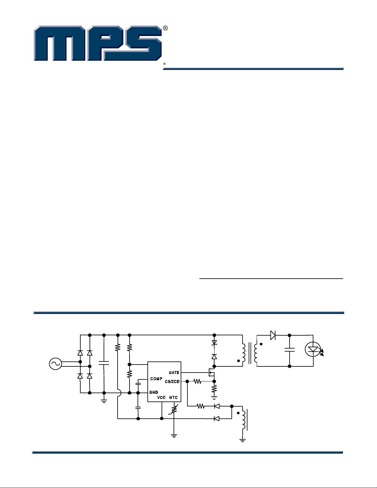
The MP4027 is a primary-side-control, offline
LED lighting controller. In a tiny TSOT23-8
package, it achieves high power factor (PF) and
accurate LED current for isolated, single-power-
stage lighting applications.
This simplifies LED-lighting-system design
significantly by eliminating the secondary-side
feedback components and the optocoupler.
The MP4027 integrates power factor correction
(PFC) and valley switching mode to reduce
MOSFET switching losses.
The MP4027 has NTC function and allows
PWM dimming.
To enhance system reliability and safety, the
MP4027 has multiple internally integrated
protection features, including over-voltage
protection (OVP), short-circuit protection (SCP),
primary-side over-current protection (OCP),
brown-out protection, over-temperature
protection (OTP), cycle-by-cycle current limit,
VCC under-voltage lockout (UVLO), and auto-
restart function.
FEATURES
Real-Current Control without Secondary-
Feedback Circuit
<2% Line/Load Regulation
NTC Thermal Current Fold-Back
PWM Dimming Available
High PF (≥0.9) over Universal Input Voltage
Valley Switching Mode for Improved
Efficiency
Brown-Out Protection
Over-Voltage Protection
Short-Circuit Protection
Over-Temperature Protection
Primary-Side Over-Current Protection
Cycle-By-Cycle Current Limit
VCC Under-Voltage Lockout Protection
Auto-Restart Function
Available in TSOT23-8 Package
APPLICATIONS
Solid-State Lighting
Industrial and Commercial Lighting
Residential Lighting
All MPS parts are lead-free and adhere to the RoHS directive. For MPS green
status, please visit MPS website under Products, Quality Assurance page.
“MPS” and “The Future of Analog IC Technology” are registered trademarks o
f
Monolithic Power Systems, Inc.
TYPICAL APPLICATION CIRCUIT
MULT
MP4027 – PRIMARY-SIDE CONTROL, OFFLINE LED CONTROLLER WITH ACTIVE PFC
MP4027 Rev. 1.02 www.MonolithicPower.com 2
12/9/2014 MPS Proprietary Information. Patent Protected. Unauthorized Photocopy and Duplication Prohibited.
© 2014 MPS. All Rights Reserved.
ORDERING INFORMATION
Part Number Package Top Marking
MP4027GJ* TSOT23-8
See Below
* For Tape & Reel, add suffix –Z (e.g. MP4027GJ–Z)
TOP MARKING
AHK: product code of MP4027GJ;
Y: year code.
PACKAGE REFERENCE
TOP VIEW
4
3
2
1
8
7
6
5
VCC
MULT
NTC
COMP
GATE
CS/ZCD
FB
GND
TSOT23-8
MP4027 – PRIMARY-SIDE CONTROL, OFFLINE LED CONTROLLER WITH ACTIVE PFC
MP4027 Rev. 1.02 www.MonolithicPower.com 3
12/9/2014 MPS Proprietary Information. Patent Protected. Unauthorized Photocopy and Duplication Prohibited.
© 2014 MPS. All Rights Reserved.
ABSOLUTE MAXIMUM RATINGS
(1)
VCC ..............................................-0.3V to +30V
GATE Drive Voltage .....................-0.3V to +17V
CS/ZCD .........................................-0.3V to 6.5V
Other Analog Inputs and Outputs ..-0.3V to 6.5V
Max. GATE Source Current....................... 0.8A
Max. GATE Sink Current ............................. -1A
Continuous Power Dissipation (T
A
= +25°C)
(2)
TSOT23-8 ................................................ 1.25W
Junction Temperature.............. -40C to +150C
Lead Temperature ....................................260°C
Storage Temperature............... -65°C to +150°C
Recommended Operating Conditions
(3)
Supply Voltage VCC .........................12V to 28V
Operating Junction Temp. (T
J
). -40°C to +125°C
Thermal Resistance
(4)
θ
JA
θ
JC
TSOT23-8………………... 100.... 55.. °C/W
Notes:
1) Exceeding these ratings may damage the device.
2) The maximum allowable power dissipation is a function of the
maximum junction temperature T
J
(MAX), the junction-to-
ambient thermal resistance θ
JA
, and the ambient temperature
T
A
. The maximum allowable continuous power dissipation at
any ambient temperature is calculated by P
D
(MAX) = (T
J
(MAX)-
T
A
)/θ
JA
. Exceeding the maximum allowable power dissipation
will cause excessive die temperature, and the regulator will go
into thermal shutdown. Internal thermal shutdown circuitry
protects the device from permanent damage.
3) The device is not guaranteed to function outside of its operating
conditions.
4) Measured on JESD51-7, 4-layer PCB.
MP4027 – PRIMARY-SIDE CONTROL, OFFLINE LED CONTROLLER WITH ACTIVE PFC
MP4027 Rev. 1.02 www.MonolithicPower.com 4
12/9/2014 MPS Proprietary Information. Patent Protected. Unauthorized Photocopy and Duplication Prohibited.
© 2014 MPS. All Rights Reserved.
ELECTRICAL CHARACTERISTICS
Typical values are at VCC = 20V, T
J
= +25°C, unless otherwise noted.
Minimum and maximum values are at VCC = 20V, T
J
= -40°C to +125°C, unless otherwise noted,
guaranteed by characterization.
Parameter Symbol Condition Min Typ Max Units
Supply Voltage
Operating Range VCC After turn on 12 28 V
Turn-On Threshold VCC
ON
VCC rising edge 23.0 25.5 28.0 V
Turn-Off Threshold VCC
OFF
VCC falling edge 8.4 9.5 11.0 V
Hysteretic Voltage VCC
HYS
14.2 15.7 17.3 V
Supply Current
Start-Up Current I
STARTUP
VCC= VCC
ON
-1V 20 50 µA
Quiescent Current I
Q
No switching 0.6 0.82 mA
Operating Current Under Fault
Condition
No switching 2 mA
Operating Current I
CC
f
s
=70kHz, C
GATE
=1nF 2 3 mA
Multiplier
Linear Operation Range V
MULT
0 3 V
Gain K
(5)
1.3 1/V
Brown-Out Protection Threshold 280 298 316 mV
Brown-Out Detection Time 25 42 60 ms
Brown-Out Protection Hysteretic
Voltage
90 100 110 mV
NTC
High-Threshold Voltage V
H_NTC
1.17 1.23 1.29 V
Low-Threshold Voltage V
L_NTC
0.67 0.77 0.87 V
Shutdown Threshold V
SD_NTC
0.355 0.39 0.425 V
Shutdown-Voltage Hysteretic
85 100 115 mV
Pull-Up Current Source I
PULL_UP
44 54 64 μA
Leakage Current I
LEAKAGE
1 μA
Error Amplifier
Reference Voltage V
REF
0.401 0.413 0.425 V
Transconductance
(6)
G
EA
125 µA/V
Upper Clamp Voltage V
COMP_H
4.5 4.75 5.1 V
Lower Clamp Voltage V
COMP_L
1.42 1.5 1.58 V
Max. Source Current
(6)
I
COMP_SOURCE
50 µA
Max. Sink Current
(6)
I
COMP_SINK
-200 µA
剩余18页未读,继续阅读
资源评论
qq_41402004
- 粉丝: 0
- 资源: 1
上传资源 快速赚钱
- 我的内容管理 展开
- 我的资源 快来上传第一个资源
- 我的收益 登录查看自己的收益
- 我的积分 登录查看自己的积分
- 我的C币 登录后查看C币余额
- 我的收藏
- 我的下载
- 下载帮助
安全验证
文档复制为VIP权益,开通VIP直接复制
信息提交成功