没有合适的资源?快使用搜索试试~ 我知道了~
TPS62046中文资料
资源推荐
资源详情
资源评论
SLVS463A − JUNE 2003 − REVISED OCTOBER 2003
FEATURES
D Up to 95% Conversion Efficiency
D Typical Quiescent Current: 18 µA
D Load Current: 1.2 A
D Operating Input Voltage Range: 2.5 V to 6.0 V
D Switching Frequency: 1.25 MHz
D Adjustable and Fixed Output Voltage
D Power Save Mode Operation at Light load
Currents
D 100% Duty Cycle for Lowest Dropout
D Internal Softstart
D Dynamic Output Voltage Positioning
D Thermal Shutdown
D Short-Circuit Protection
D 10 Pin MSOP PowerPad Package
D 10 Pin QFN 3 X 3 mm Package
APPLICATIONS
D PDA, Pocket PC and Smart Phones
D USB Powered Modems
D CPUs and DSPs
D PC Cards and Notebooks
D xDSL Applications
D Standard 5-V to 3.3-V Conversion
DESCRIPTION
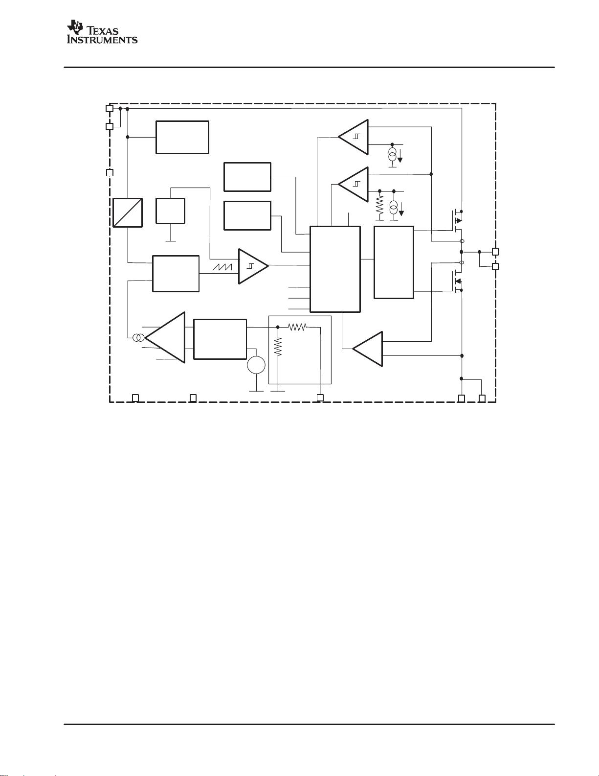
The TPS6204x family of devices are high efficiency
synchronous step-down dc-dc converters optimized for
battery powered portable applications. The devices are
ideal for portable applications powered by a single Li-Ion
battery cell or by 3-cell NiMH/NiCd batteries. With an
output voltage range from 6.0 V down to 0.7 V, the devices
support low voltage DSPs and processors in PDAs,
pocket PCs, as well as notebooks and subnotebook
computers. The TPS6204x operates at a fixed switching
frequency of 1.25 MHz and enters the power save mode
operation at light load currents to maintain high efficiency
over the entire load current range. For low noise
applications, the devices can be forced into fixed
frequency PWM mode by pulling the MODE pin high. The
TPS6204x supports up to 1.2-A load current.
7
VIN
VIN
EN
MODE
SW
FB
PGND
PGND
SW
GND
2
3
1
4
9
10
5
8
6
TPS6204x
V
I
2.5 V to 6 V
V
O
0.7 V to V
I
/1.2 A
C2
22 µF
C1
22 µF
L1
6.2 µH
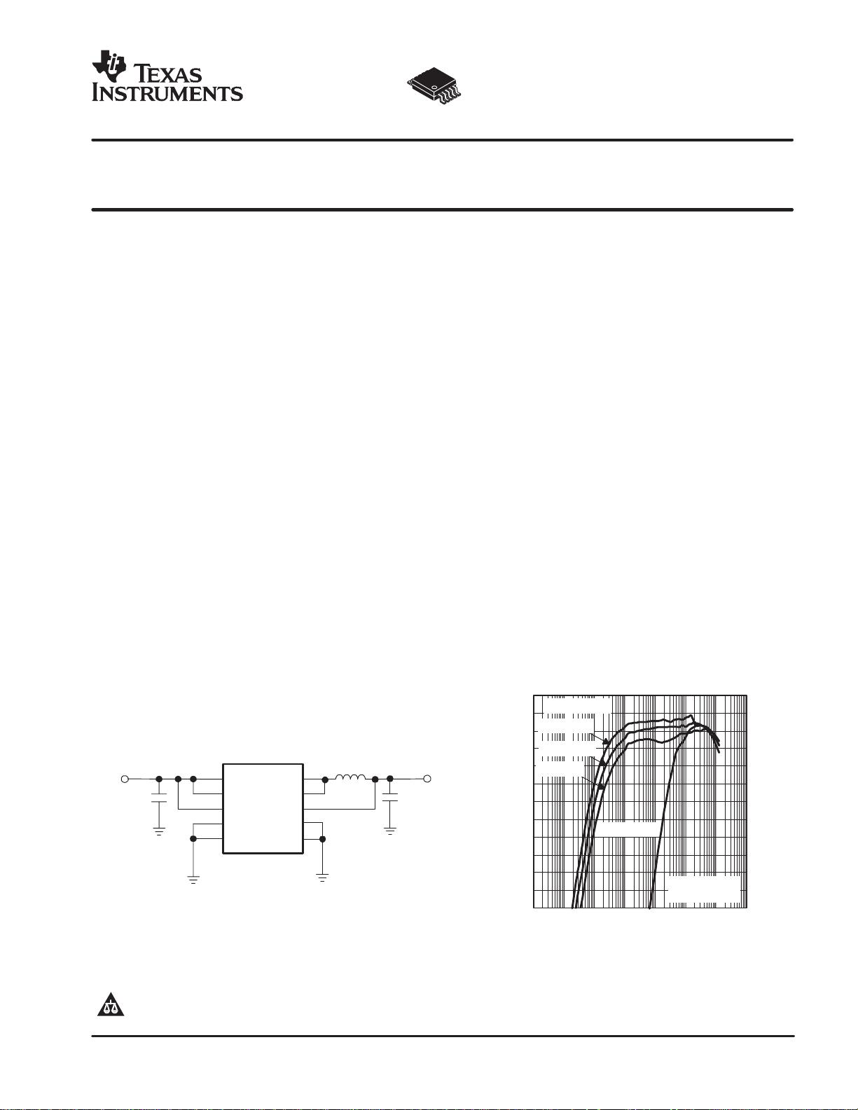
Typical Application Circuit 1.2-A Output Current
40
45
50
55
60
65
70
75
80
85
90
95
100
0 0.01 0.1 1 10 100 1 k 10 k
V
I
= 2.7 V
V
I
= 3.6 V
V
I
= 5 V
MODE = Low
V
I
= 3.6 V
MODE = High
Efficiency − %
EFFICIENCY
vs
LOAD CURRENT
I
L
− Load Current − mA
V
O
= 1.8 V
!"#$%&'(!$" !) *+%%,"( ') $# -+./!*'(!$" 0'(, %$0+*()
*$"#$%& ($ )-,*!#!*'(!$") -,% (1, (,%&) $# ,2') ")(%+&,"() )('"0'%0 3'%%'"(4
%$0+*(!$" -%$*,))!"5 0$,) "$( ",*,))'%!/4 !"*/+0, (,)(!"5 $# '// -'%'&,(,%)
Please be aware that an important notice concerning availability, standard warranty, and use in critical applications of Texas Instruments
semiconductor products and disclaimers thereto appears at the end of this data sheet.
www.ti.com
Copyright 2003, Texas Instruments Incorporated
PowerPAD is a trademark of Texas Instruments.
元器件交易网www.cecb2b.com
SLVS463A − JUNE 2003 − REVISED OCTOBER 2003
www.ti.com
2
These devices have limited built-in ESD protection. The leads should be shorted together or the device placed in conductive foam during
storage or handling to prevent electrostatic damage to the MOS gates.
ORDERING INFORMATION
T
A
VOLTAGE OPTIONS
PACKAGE PACKAGE MARKING
T
A
VOLTAGE OPTIONS
MSOP
(1)
QFN
(2)
MSOP QFN
Adjustable TPS62040DGQ TPS62040DRC BBI BBO
1.5 V TPS62042DGQ TPS62042DRC BBL BBS
−40°C to 85°C
1.6 V TPS62043DGQ TPS62043DRC BBM BBT
−40 C to 85 C
1.8 V TPS62044DGQ TPS62044DRC BBN BBU
3.3 V TPS62046DGQ TPS62046DRC BBQ BBW
(1)
The DGQ package is available in tape and reel. Add R suffix (DGQR) to order quantities of 2500 parts per reel.
(2)
The DRC package is available in tape and reel. Add R suffix (DRCR) to order quantities of 3000 parts per reel.
ABSOLUTE MAXIMUM RATINGS
over operating free-air temperature range unless otherwise noted
(1)
UNITS
Supply voltage VIN
(2)
−0.3 V to 7 V
Voltages on EN, MODE, FB, SW
(2)
−0.3 V to V
CC
+0.3 V
Continuous power dissipation See Dissipation Rating Table
Operating junction temperature range −40°C to 150°C
Storage temperature range −65°C to 150°C
Lead temperature (soldering, 10 sec) 260°C
(1)
Stresses beyond those listed under “absolute maximum ratings” may cause permanent damage to the device. These are stress ratings only, and
functional operation of the device at these or any other conditions beyond those indicated under recommended operating conditions is not implied.
Exposure to absolute-maximum-rated conditions for extended periods may affect device reliability.
(2)
All voltage values are with respect to network ground terminal.
PACKAGE DISSIPATION RATINGS
PACKAGE R
QJA
(1)
T
A
≤ 25°C
POWER RATING
T
A
= 70°C
POWER RATING
T
A
= 85°C
POWER RATING
MSOP 60°C/W 1.67 W 917 mW 667 mW
QFN 48.7°C/W 2.05 W 1.13 W 821 mW
(1)
The thermal resistance, R
ΘJA
is based on a soldered PowerPAD using thermal vias.
RECOMMENDED OPERATING CONDITIONS
MIN TYP MAX UNIT
V
I
Supply voltage 2.5 6.0 V
V
O
Output voltage range for adjustable output voltage version 0.7 V
I
V
I
O
Output current 1.2 A
L Inductor
(1)
6.2 µH
C
I
Input capacitor
(1)
22 µF
C
O
Output capacitor
(1)
22 µF
T
A
Operating ambient temperature −40 85 °C
T
J
Operating junction temperature −40 125 °C
(1)
Refer to application section for further information
元器件交易网www.cecb2b.com
SLVS463A − JUNE 2003 − REVISED OCTOBER 2003
www.ti.com
3
ELECTRICAL CHARACTERISTICS
V
I
= 3.6 V, V
O
= 1.8 V, I
O
= 600 mA, EN = VIN, T
A
= −40°C to 85°C
,
typical values are at T
A
= 25°C (unless otherwise noted)
(1)
SUPPLY CURRENT
PARAMETER TEST CONDITIONS MIN TYP MAX UNIT
V
I
Input voltage range 2.5 6.0 V
I
(Q)
Operating quiescent current I
O
= 0 mA, device is not switching 18 35 µA
I
SD
Shutdown supply current EN = GND 0.1 1 µA
V
UVLO
Under−voltage lockout threshold 1.5 2.3 V
ENABLE AND MODE
V
EN
EN high level input voltage 1.4 V
V
EN
EN low level input voltage 0.4 V
I
EN
EN input bias current EN = GND or VIN 0.01 1.0 µA
V
(MODE)
MODE high level input voltage 1.4 V
V
(MODE)
MODE low level input voltage 0.4 V
I
(MODE)
MODE input bias current MODE = GND or VIN 0.01 1.0 µA
POWER SWITCH
r
DS(ON)
P-channel MOSFET on−resistance V
I
= V
GS
= 3.6 V 115 210 mΩ
r
DS(ON)
P-channel MOSFET on−resistance V
I
= V
GS
= 2.5 V 145 270 mΩ
I
lkg(P)
P-channel leakage current V
DS
= 6.0 V 1 µA
r
DS(ON)
N-channel MOSFET on−resistance V
I
= V
GS
= 3.6 V 85 200 mΩ
r
DS(ON)
N-channel MOSFET on−resistance V
I
= V
GS
= 2.5 V 115 280 mΩ
I
Ikg(N)
N-channel leakage current V
DS
= 6.0 V 1 µA
I
L
P-channel current limit 2.5 V < V
I
< 6.0 V 1.5 1.85 2.2 A
Thermal shutdown 150 °C
OSCILLATOR
f
S
Oscillator frequency
V
FB
= 0.5 V 1 1.25 1.5 MHz
f
S
Oscillator frequency
V
FB
= 0 V 625 kHz
OUTPUT
V
O
Adjustable output voltage range TPS62040 0.7 V
IN
V
V
ref
Reference voltage 0.5 V
V
FB
Feedback voltage
TPS62040
Adjustable
V
I
= 2.5 V to 6.0 V; I
O
= 0 mA
V
I
= 2.5 V to 6.0 V; 0 mA ≤ I
O
≤ 1.2 A
0%
−3%
3%
3%
TPS62042
1.5V
V
I
= 2.5 V to 6.0 V; I
O
= 0 mA
V
I
= 2.5 V to 6.0 V; 0 mA ≤ I
O
≤ 1.2 A
0%
−3%
3%
3%
V
O
Fixed output voltage
TPS62043
1.6V
V
I
= 2.5 V to 6.0 V; I
O
= 0 mA
V
I
= 2.5 V to 6.0 V; 0 mA ≤ I
O
≤ 1.2 A
0%
−3%
3%
3%
V
O
Fixed output voltage
TPS62044
1.8V
V
I
= 2.5 V to 6.0 V; I
O
= 0 mA
V
I
= 2.5 V to 6.0 V; 0 mA ≤ I
O
≤ 1.2 A
0%
−3%
3%
3%
TPS62046
3.3V
V
I
= 3.6 V to 6.0 V; I
O
= 0 mA
V
I
= 3.6 V to 6.0 V; 0 mA ≤ I
O
≤ 1.2 A
0%
−3%
3%
3%
Line regulation
(1)
V
I
= V
O
+ 0.5 V (min. 2.5 V) to 6.0 V,
I
O
= 10 mA
0 %/V
Load regulation
(1)
I
O
= 10 mA to 1200 mA 0 %/mA
I
Ikg(SW)
Leakage current into SW pin V
I
>V
O
, 0 V ≤ Vsw ≤ V
I
0.1 1 µA
I
Ikg(SW)
Reverse leakage current into pin SW V
I
= open; EN = GND; V
SW
= 6.0 V 0.1 1 µA
f Short circuit switching frequency V
FB
= 0 V 625 kHz
(1)
The line and load regulations are digitally controlled to assure an output voltage accuracy of ±3%.
元器件交易网www.cecb2b.com
SLVS463A − JUNE 2003 − REVISED OCTOBER 2003
www.ti.com
4
PIN ASSIGNMENTS
1
2
3
4
5
10
9
8
7
6
EN
VIN
VIN
GND
FB
PGND
PGND
SW
SW
MODE
DGQ PACKAGE
(TOP VIEW)
NOTE
:
The PowerPAD must be connected to GND.
1
2
3
4
5
10
9
8
7
6
EN
VIN
VIN
GND
FB
PGND
PGND
SW
SW
MODE
DRC PACKAGE
(TOP VIEW)
Terminal Functions
TERMINAL
I/O
DESCRIPTION
NAME NO.
I/O
DESCRIPTION
EN 1 I Enable. Pulling EN to ground forces the device into shutdown mode. Pulling EN to V
I
enables the device. EN should
not be left floating and must be terminated.
VIN 2,3 I Supply voltage input
GND 4 Analog ground
FB 5 I Feedback pin. Connect FB directly to the output if the fixed output voltage version is used. For the adjustable version
an external resistor divider is connected to this pin. The internal voltage divider is disabled for the adjustable version.
MODE 6 I Pulling the MODE pin high allows the device to be forced into fixed frequency operation. Pulling the MODE pin to low
enables the power save mode where the device operates in fixed frequency PWM mode at high load currents and
in PFM mode (pulse frequency modulation) at light load currents.
SW 7,8 I/O This is the switch pin of the converter and is connected to the drain of the internal power MOSFETs
PGND 9,10 Power ground
元器件交易网www.cecb2b.com
SLVS463A − JUNE 2003 − REVISED OCTOBER 2003
www.ti.com
5
FUNCTIONAL BLOCK DIAGRAM
FB PGND
SW
VIN
EN
Undervoltage
Lockout
Bias supply
Control Logic
+
−
LoadComparator
1.25 MHz
Oscillator
Vref = 0.5 V
Driver
Shoot−thru
Logic
P−Channel
Power MOSFET
N−Channel
Power MOSFET
R1
R2
Soft
Start
+
−
+
−
Current limit Comparator
SkipComparator
Gm
Saw Tooth
Generator
V
I
+
−
Vcomp
S
R
+
−
Comp High
Comp Low
Comp Low 2
Comp High
Comp Low
Comp Low 2
−
+
Comparator
Compensation
Ref
Ref
PGND
VIN
GNDMODE
MODE
SW
For the Adjustable Version the FB Pin Is
Directly Connected to the Gm Amplifier
元器件交易网www.cecb2b.com
剩余20页未读,继续阅读
资源评论
paynexianr
- 粉丝: 0
- 资源: 1
上传资源 快速赚钱
- 我的内容管理 展开
- 我的资源 快来上传第一个资源
- 我的收益 登录查看自己的收益
- 我的积分 登录查看自己的积分
- 我的C币 登录后查看C币余额
- 我的收藏
- 我的下载
- 下载帮助
安全验证
文档复制为VIP权益,开通VIP直接复制
信息提交成功