没有合适的资源?快使用搜索试试~ 我知道了~
tps54620 中文.pdf
需积分: 5 2 下载量 11 浏览量
2023-08-17
09:31:43
上传
评论
收藏 1.98MB PDF 举报
温馨提示
试读
46页
tps54620 中文
资源推荐
资源详情
资源评论
PH
PVIN
GND
BOOT
VSENSE
COMP
TPS54620
EN
RT/CLK
SS/TR
Exposed
Thermal
Pad
Css
Rrt
R3
C1
Cboot
Co
Lo
R1
R
2
Cin
C2
VIN
VIN
VOUT
PWRGD
Copyright © 2016, Texas Instruments Incorporated
100
95
90
85
80
75
70
65
60
55
50
Efficiency-%
0 1 2 3 4 5 6
LoadCurrent- A
8V
12V
17V
VOUT =3.3V
Fsw=480kHz
Product
Folder
Order
Now
Technical
Documents
Tools &
Software
Support &
Community
An IMPORTANT NOTICE at the end of this data sheet addresses availability, warranty, changes, use in safety-critical applications,
intellectual property matters and other important disclaimers. PRODUCTION DATA.
English Data Sheet: SLVS949
TPS54620
ZHCS308F –MAY 2009–REVISED MAY 2017
TPS54620 4.5V 至至 17V 输输入入、、6A 同同步步降降压压 SWIFT™ 转转换换器器
1
1 特特性性
1
• 集成了 26mΩ 和 19mΩ MOSFET
• 分离电源轨:PVIN 上的电压范围为 1.6V 至 17V
• 200kHz 至 1.6MHz 开关频率
• 与外部时钟同步
• 温度范围内实现0.8V±1% 电压基准
• 低至 2µA 的关断静态电流
• 单调启动至预偏置输出
• -40°C 至 150°C 工作结温范围
• 可调慢启动和电源排序
• 针对欠压及过压的电源良好输出监控
• 可调节输入欠压锁定
• 若要查看 SWIFT™ 文档,请访问
http://www.ti.com.cn/swift
• 结合使用 TPS54620 和 WEBENCH 电源设计器创
建定制设计方案
2 应应用用
• 高密度分布式电源系统
• 高性能点的负载调整
• 宽带、网络互联及光纤通信基础设施
3 说说明明
TPS54620 采用热增强型 3.50mm × 3.50mm QFN 封
装,是一款功能齐全的 17V 6A 同步降压转换器;该器
件具有高效率且集成了高侧和低侧 MOSFET,经过优
化实现小型设计。通过电流模式控制减少组件数量,同
时通过选择高开关频率缩小电感封装尺寸,从而进一步
节省空间。
输出电压启动斜坡由 SS/TR 引脚控制,可实现独立电
源运行,或者跟踪状态下的运行。此外,正确配置使能
与开漏电源良好引脚也可实现电源时序。
高侧 FET 的逐周期电流限制可在过载情况下保护器
件,并通过低侧拉电流限制防止电流失控,增强限制效
果。此外,还提供可关闭低侧 MOSFET 的低侧灌电流
限制,防止反向电流过大。裸片温度超过热关断温度
时,热关断会禁用此部件。
器器件件信信息息
(1)
器器件件型型号号 封封装装 封封装装尺尺寸寸((标标称称值值))
TPS54620 VQFN (14) 3.50mm x 3.50mm
(1) 如需了解所有可用封装,请参阅数据表末尾的可订购产品附
录。
简简化化原原理理图图 效效率率与与负负载载电电流流间间的的关关系系
2
TPS54620
ZHCS308F –MAY 2009 –REVISED MAY 2017
www.ti.com.cn
版权 © 2009–2017, Texas Instruments Incorporated
目目录录
1 特特性性.......................................................................... 1
2 应应用用.......................................................................... 1
3 说说明明.......................................................................... 1
4 修修订订历历史史记记录录 ........................................................... 2
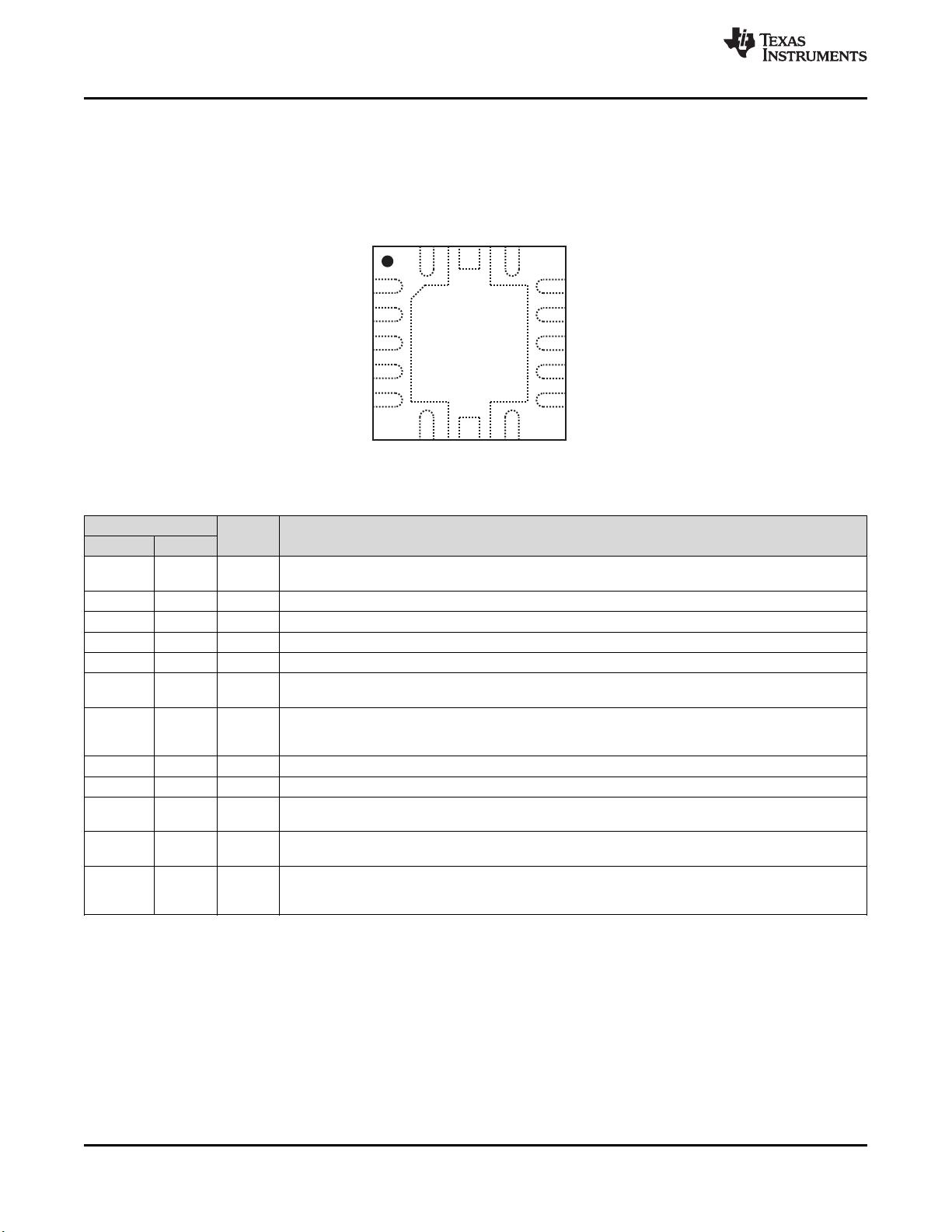
5 Pin Configurations and Functions....................... 4
6 Specifications......................................................... 5
6.1 Absolute Maximum Ratings ..................................... 5
6.2 ESD Ratings.............................................................. 5
6.3 Recommended Operating Conditions....................... 5
6.4 Thermal Information.................................................. 6
6.5 Electrical Characteristics........................................... 6
6.6 Typical Characteristics.............................................. 8
7 Detailed Description............................................ 11
7.1 Overview ................................................................. 11
7.2 Functional Block Diagram ....................................... 12
7.3 Feature Description................................................. 12
7.4 Device Functional Modes........................................ 19
8 Application and Implementation ........................ 24
8.1 Application Information............................................ 24
8.2 Typical Application ................................................. 24
9 Power Supply Recommendations...................... 34
10 Layout................................................................... 34
10.1 Layout Guidelines ................................................. 34
10.2 Layout Example .................................................... 35
10.3 Estimated Circuit Area .......................................... 36
10.4 Thermal Consideration.......................................... 36
11 器器件件和和文文档档支支持持 ..................................................... 37
11.1 器件支持................................................................ 37
11.2 接收文档更新通知 ................................................. 37
11.3 社区资源................................................................ 37
11.4 商标 ....................................................................... 37
11.5 静电放电警告......................................................... 37
11.6 Glossary................................................................ 37
12 机机械械、、封封装装和和可可订订购购信信息息....................................... 37
4 修修订订历历史史记记录录
注:之前版本的页码可能与当前版本有所不同。
Changes from Revision E (June 2016) to Revision F Page
• 将数据表文本更新至最新的文档和转换标准 ........................................................................................................................... 1
• 删除了针对 SwitcherPro™ 软件工具的全部参考,因为它不再适用于本部分 ......................................................................... 1
• Moved storage temperature ratings to the Absolute Maximum Ratings table........................................................................ 5
• Changed Handling Ratings table to ESD Ratings.................................................................................................................. 5
• Changed RHY package to RHL in the Thermal Information table ......................................................................................... 6
• Changed RGY values in the Thermal Information table......................................................................................................... 6
• Updated packages in the last bullet point of Layout Guidelines........................................................................................... 34
• Added information to the last list item in Layout Guidelines................................................................................................. 34
Changes from Revision D (October 2014) to Revision E Page
• Added recommended layout guide lines for sensitive components and the output sensing trace to the Layout
Guidelines section. ............................................................................................................................................................... 34
• 已添加
接收文档更新通知
和社区资源部分。 ........................................................................................................................ 37
Changes from Revision C (April 2011) to Revision D Page
• 增添了器件信息表、处理定额值表、建议运行条件表和热性能信息表.................................................................................... 1
• Changed the Absolute Maximum Ratings for BOOT-PH, MAX value From: 7 V To: 7.7 V .................................................. 5
• Changed Equation 28 From: C7(nF) To: C5(nF).................................................................................................................. 27
Changes from Revision B (October 2010) to Revision C Page
• Changed From separate RHL and RGY packages To a combined RHL and RGY package ................................................ 4
3
TPS54620
www.ti.com.cn
ZHCS308F –MAY 2009–REVISED MAY 2017
Copyright © 2009–2017, Texas Instruments Incorporated
Changes from Revision A (January 2010) to Revision B Page
• Changed Small Signal Model for Frequency Compensation section ................................................................................... 18
Changes from Original (May 2009) to Revision A Page
• 已更改 “具有集成 FET (SWIFT) 的 17V 输入、6A 输出同步降压开关”的原标题 .................................................................... 1
• Changed PowerPAD to Exposed Thermal Pad...................................................................................................................... 4
• Changed Changed the Absolute Maximum Ratings for EN, MAX value From: 3 V To: 6 V.................................................. 5
• Changed minimum switching frequency min value from 180 to 160...................................................................................... 7
• Changed minimum switching frequency max value from 220 to 240..................................................................................... 7
• Added "Type 3" block around C11 ....................................................................................................................................... 19
• Changed PCB Layout graphic.............................................................................................................................................. 35
13 BOOT
12 PH
11 PH
10 EN
9 SS/TR
GND 2
GND 3
PVIN 4
PVIN 5
VIN 6
7
8
1 14
RT/CLK PWRGD
VSENSE COMP
(15)
Exposed
Thermal Pad
4
TPS54620
ZHCS308F –MAY 2009 –REVISED MAY 2017
www.ti.com.cn
Copyright © 2009–2017, Texas Instruments Incorporated
(1) I = input, O = output, G = GND, P = Power
5 Pin Configurations and Functions
RHL and RGY Packages
14-Pin VQFN
(Top View)
Pin Functions
PIN
I/O
(1)
DESCRIPTION
NAME NO.
RT/CLK 1 I
Automatically selects between RT mode and CLK mode. An external timing resistor adjusts the
switching frequency of the device; in CLK mode, the device synchronizes to an external clock.
GND 2, 3 G Return for control circuitry and low-side power MOSFET.
PVIN 4, 5 P Power input. Supplies the power switches of the power converter.
VIN 6 P Supplies the control circuitry of the power converter.
VSENSE 7 I Inverting input of the gm error amplifier.
COMP 8 O
Error amplifier output, and input to the output switch current comparator. Connect frequency
compensation to this pin.
SS/TR 9 O
Slow-start and tracking. An external capacitor connected to this pin sets the internal voltage reference
rise time. The voltage on this pin overrides the internal reference. It can be used for tracking and
sequencing.
EN 10 I Enable pin. Float to enable. Adjust the input undervoltage lockout with two resistors.
PH 11, 12 O Switch node.
BOOT 13 I
A bootstrap cap is required between BOOT and PH. The voltage on this cap carries the gate drive
voltage for the high-side MOSFET.
PWRGD 14 G
Power Good fault pin. Asserts low if output voltage is low because of thermal shutdown, dropout, over-
voltage, EN shutdown, or during slow start.
Exposed
Thermal
PAD
15 G Thermal pad of the package and signal ground and it must be soldered down for proper operation.
5
TPS54620
www.ti.com.cn
ZHCS308F –MAY 2009–REVISED MAY 2017
Copyright © 2009–2017, Texas Instruments Incorporated
(1) Stresses beyond those listed under Absolute Maximum Ratings may cause permanent damage to the device. These are stress ratings
only, which do not imply functional operation of the device at these or any other conditions beyond those indicated under Recommended
Operating Conditions. Exposure to absolute-maximum-rated conditions for extended periods may affect device reliability.
6 Specifications
6.1 Absolute Maximum Ratings
(1)
MIN MAX UNIT
Input voltage
VIN –0.3 20 V
PVIN –0.3 20 V
EN –0.3 6 V
BOOT –0.3 27 V
VSENSE –0.3 3 V
COMP –0.3 3 V
PWRGD –0.3 6 V
SS/TR –0.3 3 V
RT/CLK –0.3 6 V
Output voltage
BOOT-PH 0 7.7 V
PH –1 20 V
PH 10ns Transient –3 20 V
Vdiff (GND to exposed thermal pad) –0.2 0.2 V
Source current
RT/CLK ±100 µA
PH Current Limit A
Sink current
PH Current Limit A
PVIN Current Limit A
COMP ±200 µA
PWRGD –0.1 5 mA
Operating junction temperature –40 150 °C
Storage temperature, T
stg
–65 150 °C
(1) JEDEC document JEP155 states that 500-V HBM allows safe manufacturing with a standard ESD control process.
(2) JEDEC document JEP157 states that 250-V CDM allows safe manufacturing with a standard ESD control process.
6.2 ESD Ratings
VALUE UNIT
V
(ESD)
Electrostatic discharge
Human-body model (HBM), per ANSI/ESDA/JEDEC JS-001
(1)
±2000
V
Charged-device model (CDM), per JEDEC specification JESD22-
C101
(2)
±500
6.3 Recommended Operating Conditions
over operating free-air temperature range (unless otherwise noted)
MIN NOM MAX UNIT
VIN Input voltage 4.5 17 V
PVIN Power stage input voltage 1.6 17 V
Output current 0 6 A
T
J
Operating junction temperature –40 150 °C
剩余45页未读,继续阅读
资源评论
qq_wh2020
- 粉丝: 19
- 资源: 115
上传资源 快速赚钱
- 我的内容管理 展开
- 我的资源 快来上传第一个资源
- 我的收益 登录查看自己的收益
- 我的积分 登录查看自己的积分
- 我的C币 登录后查看C币余额
- 我的收藏
- 我的下载
- 下载帮助
安全验证
文档复制为VIP权益,开通VIP直接复制
信息提交成功