没有合适的资源?快使用搜索试试~ 我知道了~
The IEEE Journal of Solid-State Circuits publishes papers each month in the broad area of solid-state circuits with particular emphasis on transistor-level design of integrated circuits.
资源推荐
资源详情
资源评论

FEBRUARY 2020
VOLUME 55
NUMBER 2
IJSCBC
(ISSN 0018-9200)
REGULAR PAPERS
A 6.5–8.1-GHz Communication/Ranging VWB Transceiver for Secure Wireless Connectivity With Enhanced
Bandwidth Efficiency and Energy Detection ................ H. Song, D. Liu, Y. Zhang, W. Rhee, and Z. Wang
219
A CMOS 76–81-GHz 2-TX 3-RX FMCW Radar Transceiver Based on Mixed-Mode PLL Chirp Generator ..........
........................................ T. Ma, W. Deng, Z. Chen, J. Wu, W. Zheng, S. Wang, N. Qi, Y. Liu, and B. Chi
233
A Batteryless Padless Crystalless 116 μm ×116 μm “Dielet” Near-Field Radio With On-Chip Coil Antenna ........
........................................................ B. Zhao, N.-C. Kuo, B. Liu, Y.-A. Li, L. Iotti, and A. M. Niknejad
249
A Reconfigurable Spectrum-Compressing Receiver for Non-Contiguous Carrier Aggregation in CMOS SOI ..........
.................................................................. H. AlShammary, A. Hamza, C. Hill, an d J. F. Buckwalter
261
High Linearity Transmit Power Mixers Using Baseband Current Feedback ...... M. V. Praveen and N. Krishnapura 272
A CMOS Two-Element 170-GHz Fundamental-Frequency Transmitter With Direct RF-8PSK Modulation ............
.......................................................................................... P. Nazari, S. Jafarlou, and P. Heydari
282
An Event-Driven Quasi-Level-Crossing Delta Modulator Based on Residue Quantization ................................
................................................................................. H. Wang, F. Schembari, and R. B. Staszewski
298
A 12.5-MHz Bandwidth 77-dB SNDR SAR-Assisted Noise Shaping Pipeline ADC .......................................
.............................................................................. Y. Song, C.-H. Chan, Y. Zhu, and R. P. Martins
312
A Temperature-Stabilized Single-Channel 1-GS/s 60-dB SNDR SAR-Assisted Pipelined ADC With Dynamic
Gm-R-Based Amplifier ................................... W. Jiang, Y. Zhu, M. Zhang, C.-H. Chan, and R. P. Martins
322
A Discrete-Time Audio Modulator Using Dynamic Amplifier With Speed Enhancement and Flicker Noise
Reduction Techniques .......................................................... S.Ma,L.Liu,T.Fang,J.Liu,andN.Wu
333
A 76.6-dB-SNDR 50-MHz-BW 29.2-mW Multi-Bit CT Sturdy MASH With DAC Non-Linearity Tolerance ..........
...................................................... L. Qi, A. Jain, D. Jiang, S.-W. Sin, R. P. Martins, and M. Ortmanns
344
A Second-Order Purely VCO-Based CT ADC Using a Modified DPLL Structure in 40-nm CMOS ..............
............................................................ Y. Zhong, S. Li, X. Tang, L. Shen, W. Zhao, S. Wu, and N. Sun
356
A BJT-Based Temperature-to-Digital Converter With a ±0.25
◦
C3σ -Inaccuracy From −40
◦
Cto+180
◦
CUsing
Heater-Assisted Voltage Calibration .............................................. B. Yousefzadeh and K. A. A. Makinwa
369
A 0.3 lx–1.4 Mlx Monolithic Silicon Nanowire Light-to-Digital Converter With Temperature-Independent Offset
Cancellation ..................................................................................... C. Rhee, J. Park, and S. Kim
378
Combined In-Pixel Linear and Single-Photon Avalanche Diode Operation With Integrated Biasing for
Wide-Dynamic-Range Optical Sensing ........................................... H. Ouh, B. Shen, and M. L. Johnston
392
A 10-mA LDO With 16-nA IQ and Operating From 800-mV Supply .......... N. Adorni, S. Stanzione, and A. Boni 404
A 13.9-nA ECG Amplifier Achieving 0.86/0.99 NEF/PEF Using AC-Coupled OTA-Stacking ...........................
........................................................................................................ S. Mondal and D. A. Hall
414

A 951-fs
rms
Period Jitter 3.2% Modulation Range In-Band Modulation Spread-Spectrum Clock Generator ............
.............................................................. H. Sun, K. Sobue, K. Hamashita, T. Anand, and U.-K. Moon
426
A 32-Gb/s Simultaneous Bidirectional Source-Synchronous Transceiver With Adaptive Echo Cancellation
Techniques .......................... Y.-H. Fan, A. Kumar, T. Iwai, A. Roshan-Zamir, S. Cai, B. Sun, and S. Palermo
439
A 1.9-mW SVM Processor With On-Chip Active Learning for Epileptic Seizure Control ................................
..................................................................... S.-A. Huang, K.-C. Chang, H.-H. Liou, and C.-H. Yang
452
STICKER: An Energy-Efficient Multi-Sparsity Compatible Accelerator for Convolutional Neural Networks in 65-nm
CMOS ............................... Z. Yuan, Y. Liu, J. Yue, Y. Yang, J. Wang, X. Feng, J. Zhao, X. Li, and H. Yang
465
Enhanced Power and Electromagnetic SCA Resistance of Encryption Engines via a Security-Aware Integrated
All-Digital LDO ...... A. Singh, M. Kar, V. C. K. Chekuri, S. K. Mathew, A. Rajan, V. De, and S. Mukhopadhyay
478
Computationally Enabled Minimum Total Energy Tracking for a Performance Regulated Sub-Threshold Microprocessor
in 65-nm CMOS ................................................................ F. ur Rahman, R. Pamula, and V. S. Sathe
494
A 2.92-Gb/s/W and 0.43-Gb/s/MG Flexible and Scalable CGRA-Based Baseband Processor for Massive MIMO
Detection ...................................................................... G. Peng, L. Liu, S. Zhou, S. Yin, and S. Wei
505

378 IEEE JOURNAL OF SOLID-STATE CIRCUITS, VOL. 55, NO. 2, FEBRUARY 2020
A 0.3 lx–1.4 Mlx Monolithic Silicon Nanowire
Light-to-Digital Converter With
Temperature-Independent Offset Cancellation
Cyuyeol Rhee , Junyoung Park, Student Member, IEEE, and Suhwan Kim , Senior Member, IEEE
Abstract—This article presents a monolithic light-to-digital
converter (LDC) based on silicon nanowires. The silicon
nanowires are arranged in a configuration, which allows can-
cellation for the offset due to dark leakage current and facil-
itates system-level chopping of the signal chain, including the
nanowires. The readout integrated circuit (ROIC) has an ana-
log front end (AFE) with a resistive-feedback transimpedance
amplifier (TIA) to provide a constant voltage that strongly
biases the nanowires. A programmable-gain switched-capacitor
incremental delta–sigma analog-to-digital converter doubles the
output of the TIA and feeds a digital back end that provides
a decimated output. Finally, system-level chopping reduces the
residual offset and 1/f noise, and 50-/60-Hz rejection suppresses
interference from mains lighting. Fabricated in a 0.18-µmCMOS
process, the LDC has an input-referred current noise density
of 235 fA/
√
Hz, and a dynamic range of 106.7, from 0.3 lx to
1.4 Mlx. The offset from the nanowires and the AFE is reduced
to less than 30 µV and offset drift of 193 nV/°C in a temperature
range of −40 °C–85 °C. The AFE of the LDC draws 59.5 µAat
3.3 V, and the digital back end draws 8 µAat1.8V.
Index Terms— 1/f noise, 50-/60-Hz rejection, dark leakage
current, light-to-digital converter (LDC), programmable-gain
incremental delta–sigma analog-to-digital converter (ADC),
silicon nanowires, system-level chopping.
I. INTRODUCTION
L
IGHT sensor systems are used in a variety of applications,
such as light energy monitoring, proximity detection,
and non-invasive physiological monitoring [1]–[5]. A light
sensor system, which usually consists of a photodetector and
a readout integrated circuit (ROIC), must be able to handle
a wide range of illumination conditions from a very dark
environment (<1 lx) to bright sunlight (∼1 Mlx) [1], [2].
A light sensor system is usually based on a photodiode
(PD) [1]–[5]. This type of photodetector is widely used
because it has high linearity and is relatively insensitive to
changes in bias voltages. However, PDs require an illumination
area of several square millimeters due to their relatively
low photoresponsivity, making them less suitable for use in
Manuscript received March 15, 2019; revised July 5, 2019 and
September 16, 2019; accepted October 12, 2019. Date of publication
November 7, 2019; date of current version January 28, 2020. This article
was approved by Associate Editor David Stoppa. (Corresponding author:
Suhwan Kim.)
The authors are with the Department of Electrical and Computer Engi-
neering, Seoul National University, Seoul 08826, South Korea, and also
with the Inter-University Semiconductor Research Center (ISRC), College of
Engineering, Seoul 151-742, South Korea (e-mail: suhwan@snu.ac.kr).
Color versions of one or more of the figures in this article are available
online at http://ieeexplore.ieee.org.
Digital Object Identifier 10.1109/JSSC.2019.2949257
ROICs [6]. Other types of photodetector can be integrated
into a system on a chip. For example, an array of single-
photon avalanche diodes (SPADs) with a very small area
(∼0.00072 mm
2
) and high photosensitivity has been integrated
into an ROIC [7]–[9]. However, SPADs require a high voltage
between 8 and 20 V, which involves an extra charge pump,
which increases power consumption [8]–[10], and the sys-
tem with SPADs provides a limited optical dynamic range
of 48 dB [8]. Silicon nanowires do not require high-voltage
biasing, high sensitivity to light and the high surface-to-
volume ratio [6], [11], [12], and, therefore, emerged as a very
promising photodetector.
Light falling on a silicon nanowire creates electron–hole
pairs, and thus, its resistance decreases [6]. This response
is monotonic, but the resulting photocurrent depends on the
voltage applied to the nanowire [6], [11]. A nanowire, which
is not illuminated at all, still has a finite resistance, and if
the voltage is applied, the current will flow. This is called the
dark leakage current. The equivalent resistance of a silicon
nanowire at a specific bias voltage varies with temperature,
even in very low illumination [14], [17], which means that
the offset arising from the dark leakage current is sensitive
to temperature. When silicon nanowires are integrated with
other circuits, this current can be affected by waste heat
from other circuits, as well as the ambient temperature. The
offsets produced not only by the dark leakage current but also
by the ROIC are generally undesirable and are cumbersome
when temperature changes because a one-time calibration is
not enough to eliminate offset errors across all temperature.
Therefore, these offsets must be suppressed over the operating
temperature range.
To overcome these issues, we present a monolithic light-
to-digital converter (LDC), which compensates for the offset
voltages generated by dark leakage current and ROIC, over
its entire temperature range. This LDC consists of a silicon
nanowire sensor (R
S
), a dark cell (R
D
), an analog front end
(AFE), a digital back end, and peripheral blocks. The AFE,
which largely determines the performance of the LDC, con-
sists of a resistive-feedback transimpedance amplifier (TIA)
and a programmable-gain switched-capacitor (SC) incremental
delta–sigma () analog-to-digital modulator. Within the
TIA, a chopping technique is combined with a ripple-reduction
loop (RRL) to achieve constant biasing of the sensor, low
1/ f noise corner, and a reduced offset. This TIA operates
in conjunction with system-level chopping, which takes place
0018-9200 © 2019 IEEE. Personal use is permitted, but republication/redistribution requires IEEE permission.
See http://www.ieee.org/publications_standards/publications/rights/index.html for more information.

RHEE et al.: 0.3 lx–1.4 Mlx MONOLITHIC SILICON NANOWIRE LDC WITH TEMPERATURE-INDEPENDENT OFFSET CANCELLATION 379
across the entire system, including the sensor, to eliminate
the offset due to dark leakage current and the ROIC, across
the operating temperature range. System-level chopping also
reduces the residual 1/ f noise and sensor bias voltage. This
eliminates the need for offset calibration when the sensor is
interfaced with the ROIC. A digital rejection filter notches out
50-/60-Hz noise from any mains light source.
The remainder of this article is organized as follows.
In Section II, we describe silicon nanowires. In Section III,
we introduce the LDC. Section IV is devoted to the details of
the TIA. In Section V, we introduce the programmable-gain
SC incremental analog-to-digital converter (ADC). Exper-
imental results are presented in Section VI. We draw conclu-
sions in Section VII.
II. S
ILICON NANOWIRESASALIGHT-SENSING ELEMENT
Silicon nanowires can be constructed by bottom–up or
top–down fabrication. Bottom–up fabrication is synthesis-
based, which is incompatible with the standard process of
CMOS ICs [15], [16]. In this case, nanowires and ICs must
be connected by wire bonding, resulting in a high packaging
cost. A sensing system created in this manner would be
large and noisy due to the parasitic capacitance formed by
the bonding process. An integrated configuration of silicon
nanowires can be produced by top–down fabrication, such as
photolithography and etching [6], [13]–[16].
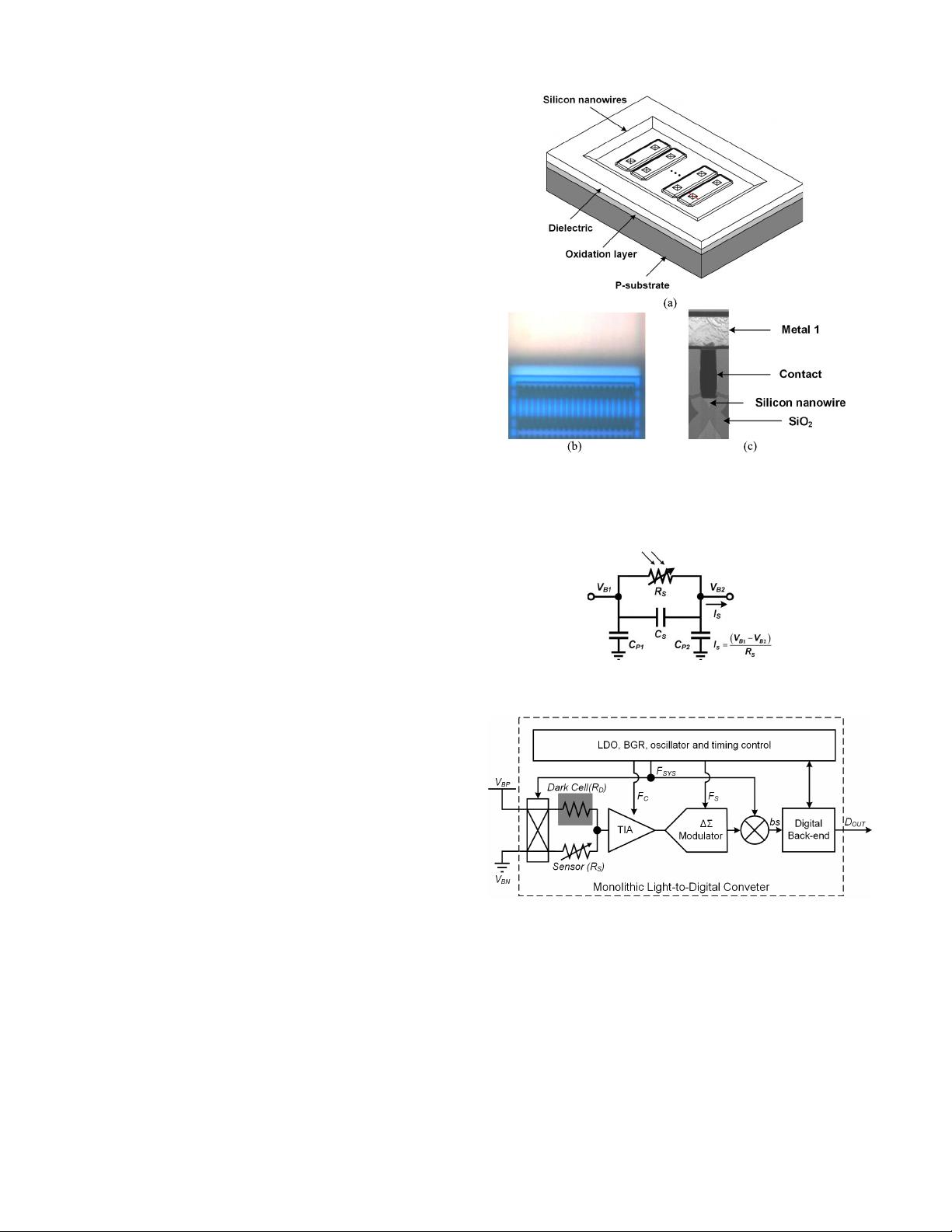
Within a CMOS standard process, silicon nanowires, such
as that shown in Fig. 1(a) and (b), can be produced by
the following fabrication process. A p-type substrate lightly
doped with boron is prepared, and thermal oxide is grown
by a wet oxidation process. Line patterns of 0.5 μmare
defined by a photolithography process, and rectangular sil-
icon columns are fabricated by silicon reactive ion etching
process. Afterward, a wet etching process using tetramethy-
lammonium hydroxide (TMAH) solution forms hour-glass-
shaped structures. In this process, anisotropic wet etching is
performed utilizing that the etch rate of (111)-plane is more
than one hundred times slower than that of the (100)-plane.
Then, the second wet oxidation process is performed to fabri-
cate triangular-shaped silicon nanowires by thermal oxidation.
Gaps between the silicon nanowires are filled with oxida-
tion layer by high-density plasma chemical vapor deposition
(HDPCVD). Silicon nanowires are covered with oxide and
nitride passivation layer. After fabrication of silicon nanowires,
CMOS circuits are processed. The CMOS process provides
four interconnect layers (metal 1 –metal 4). The dark cell is
shielded by placing the metals available in the CMOS process
on the top of the dark cell [18]–[22]. Fig. 1(c) is a scanning
transmission electron microscope (STEM) image of a silicon
nanowire with a width of 300 nm. Fig. 2 is the equivalent
electrical model of the sensor, which is an array of silicon
nanowires. The model consists of an equivalent resistance R
S
,
a shunt capacitance C
S
, and two parasitic capacitances C
P1
and C
P2
due to interconnections to the terminals of the silicon
nanowires. Rs decreases from a few G down to 11 M as
the light intensity changes from 0 lx to 28 000 lx. C
S
can be
ignored in a relatively slow system, which is likely to have
Fig. 1. (a) Arrangement of CMOS-compatible silicon nanowires in an array.
Metal connections to contact holes are not shown. (b) Top view of an array of
silicon nanowires and the dark cell (white). (c) STEM image of the vertical
cross section view [dashed line in Fig. 1(a)] of a silicon nanowire.
Fig. 2. Electrical model of the silicon nanowire sensor.
Fig. 3. Monolithic silicon nanowire LDC.
a bandwidth below 10 Hz. On-chip integration of the sensor
and the ROIC can keep the values of C
P1
and C
P2
smaller
than a few hundred femtofarads.
III. M
ONOLITHIC LDC
The LDC shown in Fig. 3 consists of a silicon nanowire
sensor, a dark cell, a TIA, an incremental modulator,
a digital back end, and peripherals, such as a bandgap voltage
reference (BGR), a low-dropout (LDO) voltage regulator, and
an oscillator. The sensor R
S
is an array of silicon nanowires,

380 IEEE JOURNAL OF SOLID-STATE CIRCUITS, VOL. 55, NO. 2, FEBRUARY 2020
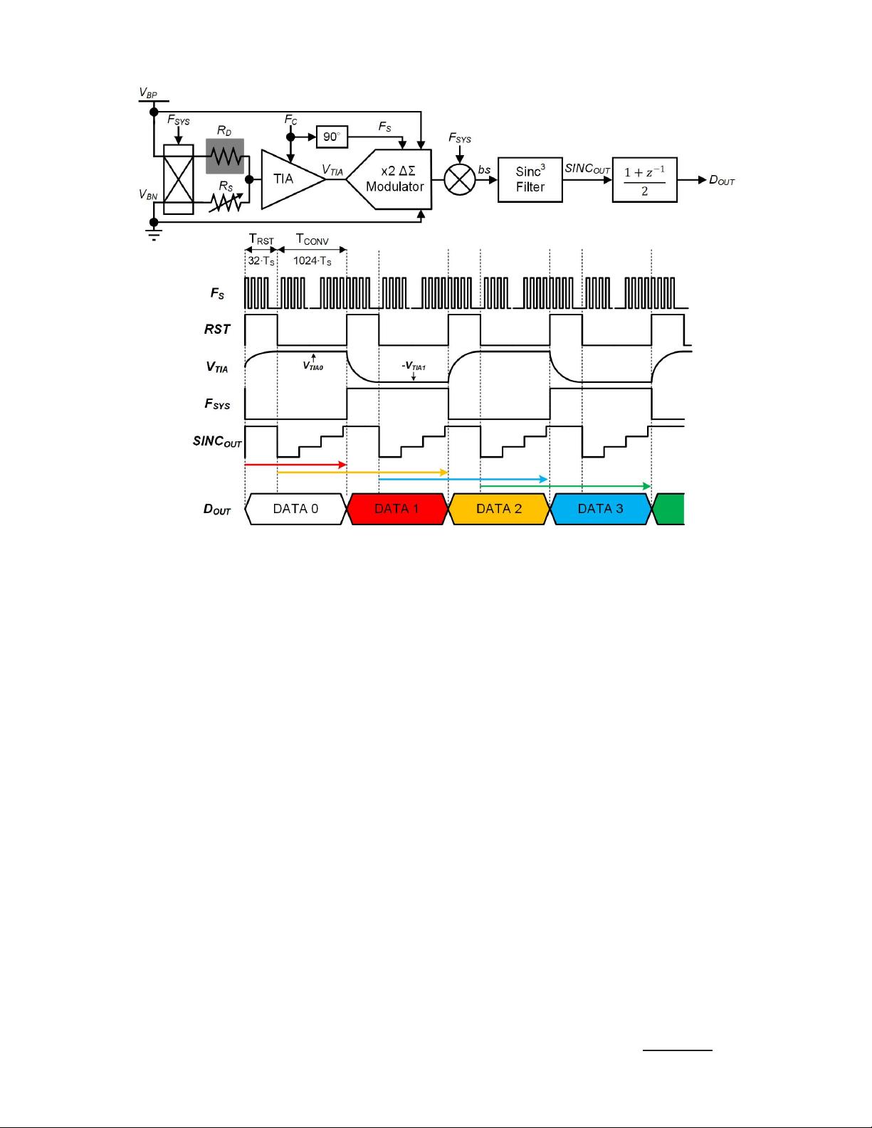
Fig. 4. Architecture of the analog front end and its timing diagram.
and the dark cell R
D
is a duplicate of the sensor, except that it
is covered and surrounded by metal layers. There is chopping
on the entire system from sensor bias voltages to the output
of the modulator by F
SYS
, and a decimation filter decimates
the modulator’s output bs and provides a robust rejection
capability. The decimated 18-bit digital codes D
OUT
are passed
through a serial communication in the digital back end. The
internal oscillator generates a 4-MHz clock signal for I
2
C and
SPI for serial communications. The clock generator receives an
86.4-kHz clock signal from the digital back end and generates
a 21.6-kHz clock signal F
C
for chopping the main amplifier
in the TIA and the RRL and 90° shifted sampling clock
signal F
S
for the modulator. A voltage V
BP
of 3.3 V
biases the sensor and provides the reference voltage to the
modulator. The BGR and LDO generate 1.8-V supply
for the digital circuits. A biasing circuit distributes a current
of 200 nA to bias amplifiers in the TIA and the modulator.
The system can save energy by going into sleep mode after a
conversion. The power-on reset (POR) puts the system into a
known state after wakeup.
The architecture of the AFE and its timing diagram are
shown in Fig. 4. The transimpedance gain of the TIA can
be controlled from 200 k to 10 M to accommodate the
wide dynamic range of ambient light while providing sub-lx
resolution. To achieve sub-lx resolution, the AFE requires the
transimpedance gain of 10 M and a 16.5-bit ADC, with
a single-ended operation of the TIA. This corresponds to a
noise voltage of 20 μV
rms
in the band of interest. The
modulator has a gain of 2, but its integrators are not saturated
at full-scale input because the output of the TIA and the
common-mode voltage V
CM
are connected to the differential
inputs of the modulator. The noise and offset of the readout IC
are primarily suppressed by a chopping scheme in the TIA.
The chopping ripple of the input stage is suppressed by a
continuous-time RRL to provide constant biasing of the sensor.
Asinc
3
filter is used for decimation, and a finite impulse
response filter provides a moving average of the SINC
OUT
signal for system-level chopping.
IV. I
MPLEMENTATION OF THE TIA
A. Sensor Configuration
In LDCs based on PDs, a dark PD is used to cancel a sensing
PD’s dark leakage current by connecting the sensing PD to one
input of a differential TIA and a dark PD to the other input,
as shown in Fig. 5(a) [18]–[22]. Since the equivalent resistance
of a PD is large and insensitive to light intensity, the circuit
in Fig. 5(a) does not affect the input common-mode voltage
of the TIA. However, if silicon nanowires are substituted
for the PDs, as shown in Fig. 5(b), the voltage across the
sensor will vary, changing the relationship between light
intensity and current. Fig. 5(c) shows the dc common-mode
equivalent circuit if the circuit described in Fig. 5(b). The input
common-mode voltage V
IN,dc
of the amplifier would vary as
follows:
V
IN,DC
= V
TIACOM
·
R
P
R
P
+ R
F
/2
(1)
剩余302页未读,继续阅读
资源评论

netshell
- 粉丝: 11
- 资源: 185
上传资源 快速赚钱
 我的内容管理
展开
 我的资源
快来上传第一个资源
 我的收益 登录查看自己的收益
 我的积分
登录查看自己的积分
 我的C币
登录后查看C币余额
 我的收藏
我的收藏  我的下载
我的下载  下载帮助
下载帮助

 前往需求广场,查看用户热搜
最新资源
资源上传下载、课程学习等过程中有任何疑问或建议,欢迎提出宝贵意见哦~我们会及时处理!
点击此处反馈


安全验证
文档复制为VIP权益,开通VIP直接复制
 信息提交成功