
TPS552882-Q1 36V 16A 降压/升压转换器
1 特性
• 符合 AEC-Q100 标准:
– 器件温度等级 1:–40°C 至 +125°C 环境工作
温度范围
• 宽输入和输出电压范围
– 宽输入电压范围:2.7V 至 36V
– 宽输出电压范围:0.8V 至 22V
• 在整个负载范围内具有高效率
– V
IN
= 12V、V
OUT
= 20V 且 I
OUT
= 3A 时效率为
97%
• 避免频率干扰和串扰
– 可选的时钟同步
– 可编程开关频率范围为 200kHz 至 2.2MHz
• 降低 EMI
– 可选可编程扩展频谱
– 无引线封装
• 丰富的保护特性
– 输出过压保护
– 利用断续模式实现输出短路保护
– 热关断保护
– 可编程平均电感器电流限制高达 16A
• 小解决方案尺寸
– 开关频率高达 2.2MHz(最大值)
– 4.0mm × 3.5mm HotRod
™
QFN 封装
• 电缆上压降的可调输出电压补偿
• 轻负载状态下的可编程 PFM 和 FPWM 模式
• 感应电阻器的可编程输出电流限制
• ±1% 基准电压精度
• 固定 4ms 软启动时间
• 使用 TPS552882-Q1 并借助 WEBENCH
®
Power
Designer 创建定制设计方案
2 应用
• USB PD
• 汽车信息娱乐系统与仪表组
• 汽车充电器
3 说明
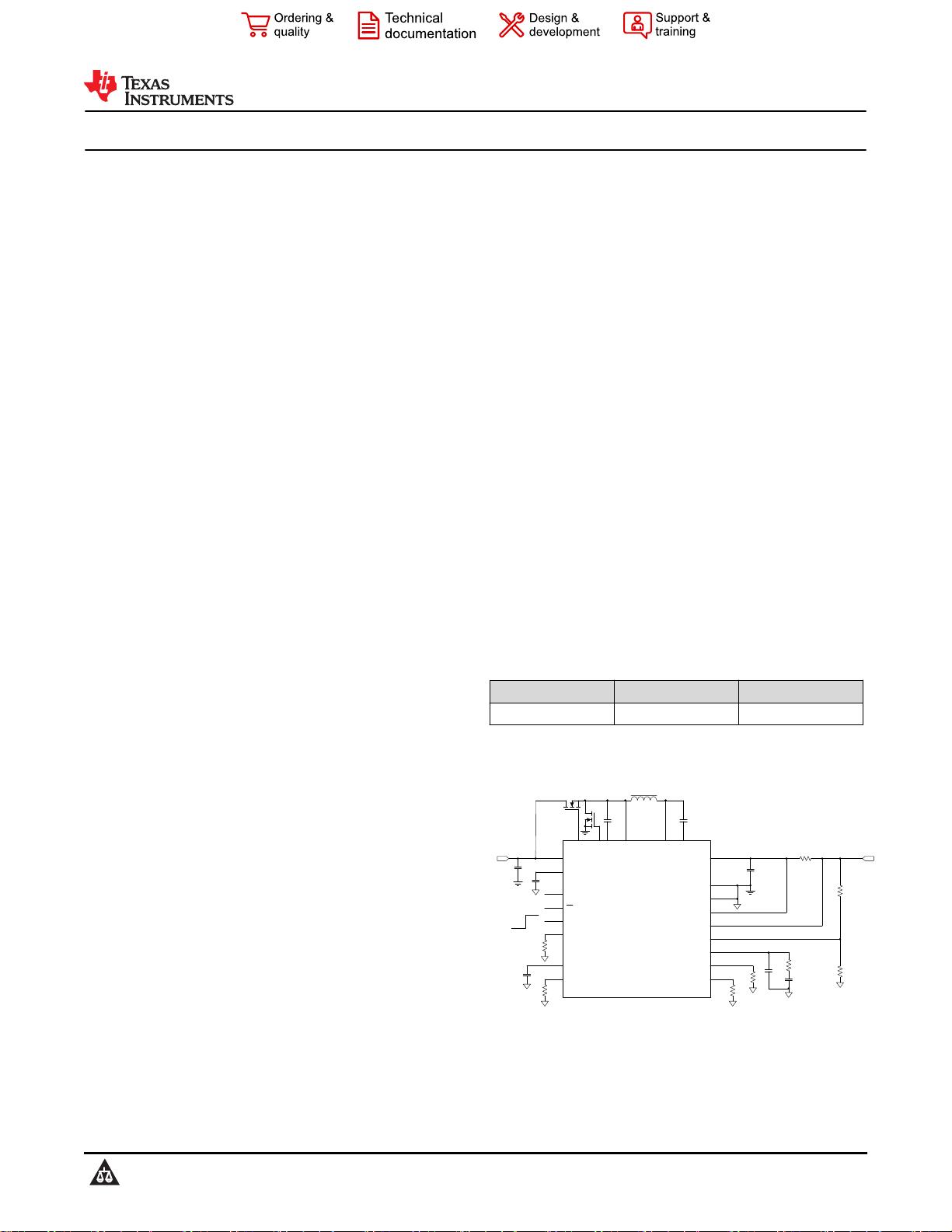
TPS552882-Q1 是一款同步四开关降压/升压转换器,
能够将输出电压稳定在等于、高于或低于输入电压的某
一电压值上。TPS552882-Q1 在 2.7V 至 36V 的宽输
入电压范围内工作,可输出 0.8V 至 22V 电压以支持各
种不同的应用。
TPS552882-Q1 集成了两个 16A MOSFET,其中的升
压腿可实现解决方案尺寸和效率间的平衡。
TPS552882-Q1 使用外部电阻分压器,通过 1.2V 内部
基准电压来设置输出电压。TPS552882-Q1 能够通过
12V 输入电压提供 100W 的功率。
TPS552882-Q1 采用平均电流模式控制方案。开关频
率可通过外部电阻在 200kHz 至 2.2MHz 之间进行编
程,并且可与外部时钟同步。TPS552882-Q1 还提供
可选的扩频,从而更大限度地减少峰值 EMI。
TPS552882-Q1 提供输出过压保护、平均电感器电流
限制、逐周期峰值电流限制和输出短路保护。
TPS552882-Q1 还使用持续过载情况下的可选输出电
流限制和断续模式保护来确保安全运行。
TPS552882-Q1 可以使用具有高开关频率的小型电感
器和电容器。此器件采用 4.0mm × 3.5mm QFN 封
装。
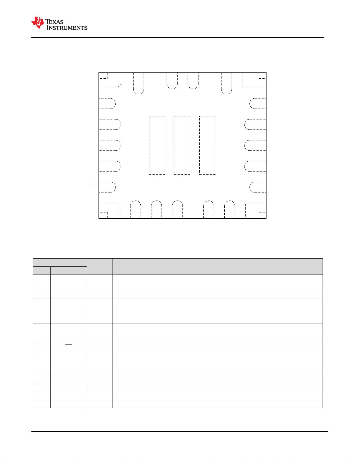
器件信息
器件型号
封装
(1)
封装尺寸
TPS552882-Q1 VQFN-HR 4.00mm × 3.50mm
(1) 如需了解所有可用封装,请参阅数据表末尾的可订购产品附
录。
DR1L
VIN
TPS552882-Q1
ILIM
VIN = 2.7V to 36V
MODE
C7
PGND
COMP
R5
R3
C2
VOUT
VOUT = 0.8V to 20V
C4
BOOT1
OFF
ON
C6
L1
4.7µH
SW2
BOOT2
DR1H
C1
AGND
C5
PG
VCC
C3
4.7µF
FSW
EN/UVLO
SW1
CDC
R4
DITH/SYNC
C8
R2
ISP
ISN
R7
10PŸ
0.1µF0.1µF
R8
FB
CC
R2
R1
典型应用电路
TPS552882-Q1
ZHCSMV3 – DECEMBER 2020
本文档旨在为方便起见,提供有关 TI 产品中文版本的信息,以确认产品的概要。有关适用的官方英文版本的最新信息,请访问
www.ti.com,其内容始终优先。TI 不保证翻译的准确性和有效性。在实际设计之前,请务必参考最新版本的英文版本。
English Data Sheet: SLVSFQ8

剩余43页未读,继续阅读
资源评论


