COMMERCIAL AND INDUSTRIAL
TEMPERATURE RANGES
IDT72T36135M 2.5V 18M-BIT TeraSync
™™
™™
™ 36-BIT FIFO
524,288 x 36
3
DESCRIPTION:
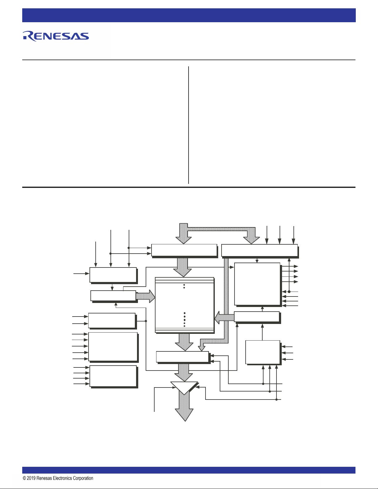
The IDT72T36135M is an exceptionally deep, extremely high speed,
CMOS First-In-First-Out (FIFO) memory with clocked read and write controls
and a wide extended x36 bus to allow ample data flow. These FIFOs offer
several key user benefits:
• High density offering of 18 Mbit
• 200MHz R/W Clocks supporting 7.2Gbps of data throughput
• User selectable MARK location for retransmit
• User selectable I/O structure for HSTL or LVTTL
• Asynchronous/Synchronous translation on the read or write ports
• The first word data latency period, from the time the first word is written
to an empty FIFO to the time it can be read, is fixed and short.
TeraSync FIFOs are particularly appropriate for network, video, telecom-
munications, data communications and other applications that need to buffer
large amounts of data at very high performance.
The input port can be selected as either a Synchronous (clocked) interface,
or Asynchronous interface. During Synchronous operation the input port is
controlled by a Write Clock (WCLK) input and a Write Enable (WEN) input. Data
present on the Dn data inputs is written into the FIFO on every rising edge of
WCLK when WEN is asserted. During Asynchronous operation only the WR
input is used to write data into the FIFO. Data is written on a rising edge of WR,
the WEN input should be tied to its active state, (LOW).
The input port can be selected for either 2.5V LVTTL or HSTL operation,
this operation is selected by the state of the WHSTL input during a master reset.
A Write Chip Select input (WCS) is provided for use when the write port is in
both LVTTL and HSTL modes. During operation the WCS input can be used
to disable write port inputs (data only).
The output port can be selected as either a Synchronous (clocked) interface,
or Asynchronous interface. During Synchronous operation the output port is
controlled by a Read Clock (RCLK) input and Read Enable (REN) input. Data
is read from the FIFO on every rising edge of RCLK when REN is asserted.
During Asynchronous operation only the RD input is used to read data from the
FIFO. Data is read on a rising edge of RD, the REN input should be tied to its
active state, LOW. When Asynchronous operation is selected on the output port
the FIFO must be configured for Standard IDT mode, also the RCS should be
tied LOW and the OE input used to provide three-state control of the outputs, Qn.
The output port can be selected for either 2.5V LVTTL or HSTL operation,
this operation is selected by the state of the RHSTL input during a master reset.
An Output Enable (OE) input is provided for three-state control of the outputs.
A Read Chip Select (RCS) input is also provided, the RCS input is synchronized
to the read clock, and also provides three-state control of the Qn data outputs.
When RCS is disabled, the data outputs will be high impedance. During
Asynchronous operation of the output port, RCS should be enabled, held LOW.
The frequencies of both the RCLK and the WCLK signals may vary from 0
to fMAX with complete independence. There are no restrictions on the frequency
of the one clock input with respect to the other.
There are two possible timing modes of operation with these devices: IDT
Standard mode and First Word Fall Through (FWFT) mode.
In IDT Standard mode, the first word written to an empty FIFO will not appear
on the data output lines unless a specific read operation is performed. A read
operation, which consists of activating REN and enabling a rising RCLK edge,
will shift the word from internal memory to the data output lines.
In FWFT mode, the first word written to an empty FIFO is clocked directly
to the data output lines after three transitions of the RCLK signal. A REN does
not have to be asserted for accessing the first word. However, subsequent
words written to the FIFO do require a LOW on REN for access. The state of
the FWFT/SI input during Master Reset determines the timing mode in use.
For applications requiring more data storage capacity than a single FIFO
can provide, the FWFT timing mode permits depth expansion by chaining FIFOs
in series (i.e. the data outputs of one FIFO are connected to the corresponding
data inputs of the next). No external logic is required.
The 18M-bit TeraSync FIFO has 8 flag pins, EF/OR[1:2] (Empty Flag or
Output Ready), FF/IR[1:2] (Full Flag or Input Ready), PAE[1:2] (Program-
mable Almost-Empty flag) and PAF[1:2] (Programmable Almost-Full flag). The
EF[1:2] and FF[1:2] functions are selected in IDT Standard mode. The IR[1:2]
and OR[1:2] functions are selected in FWFT mode. PAE[1:2] and PAF[1:2] are
always available for use, irrespective of timing mode. Each flag has a double
because the 18M FIFO was designed as a Multi-chip Module, so each set of
flags supports its respective internal 9M FIFO. Some extra external gating logic
will have to be used to accurately read each flag output. This will be covered
in the flagging section of the datasheet.
PAE[1:2] and PAF[1:2] can be programmed independently to switch at any
point in memory. Programmable offsets determine the flag switching threshold
and can be loaded by two methods: parallel or serial. Eight default offset settings
are also provided, so that PAE[1:2] can be set to switch at a predefined number
of locations from the empty boundary and the PAF[1:2] threshold can also be
set at similar predefined values from the full boundary. The default offset values
are set during Master Reset by the state of the FSEL0, FSEL1, and LD pins.
For serial programming, SEN together with LD on each rising edge of
SCLK, are used to load the offset registers via the Serial Input (SI). For parallel
programming, WEN together with LD on each rising edge of WCLK, are used
to load the offset registers via Dn. REN together with LD on each rising edge
of RCLK can be used to read the offsets in parallel from Qn regardless of whether
serial or parallel offset loading has been selected.
During Master Reset (MRS) the following events occur: the read and write
pointers are set to the first location of the FIFO. The FWFT pin selects IDT
Standard mode or FWFT mode.
The Partial Reset (PRS) also sets the read and write pointers to the first
location of the memory. However, the timing mode, programmable flag
programming method, and default or programmed offset settings existing before
Partial Reset remain unchanged. The flags are updated according to the timing
mode and offsets in effect. PRS is useful for resetting a device in mid-operation,
when reprogramming programmable flags would be undesirable.
It is also possible to select the timing mode of the PAE[1:2] (Programmable
Almost-Empty flag) and PAF[1:2] (Programmable Almost-Full flag) outputs. The
timing modes can be set to be either asynchronous or synchronous for the
PAE[1:2] and PAF[1:2] flags.
If asynchronous PAE/PAF[1:2] configuration is selected, the PAE[1:2] is
asserted LOW on the LOW-to-HIGH transition of RCLK. PAE[1:2] is reset to
HIGH on the LOW-to-HIGH transition of WCLK. Similarly, the PAF[1:2] is
asserted LOW on the LOW-to-HIGH transition of WCLK and PAF[1:2] is reset
to HIGH on the LOW-to-HIGH transition of RCLK.
If synchronous PAE/PAF[1:2] configuration is selected , the PAE[1:2] is
asserted and updated on the rising edge of RCLK only and not WCLK. Similarly,
PAF[1:2] is asserted and updated on the rising edge of WCLK only and not
RCLK. The mode desired is configured during MasterReset by the state of the
Programmable Flag Mode (PFM) pin.
This device includes a Retransmit from Mark feature that utilizes two control
inputs, MARK and , RT (Retransmit). If the MARK input is enabled with respect
to the RCLK, the memory location being read at that point will be marked. Any
subsequent retransmit operation, RT goes LOW, will reset the read pointer to
this ‘marked’ location.
If, at any time, the FIFO is not actively performing an operation, the chip will
automatically power down. Once in the power down state, the standby supply
current consumption is minimized. Initiating any operation (by activating control