没有合适的资源?快使用搜索试试~ 我知道了~
TJA1024 LIN Transceiver datasheet
需积分: 1 2 下载量 4 浏览量
2022-12-25
18:14:00
上传
评论
收藏 199KB PDF 举报
温馨提示
试读
25页
TJA1024 LIN Transceiver datasheet
资源推荐
资源详情
资源评论
1. General description
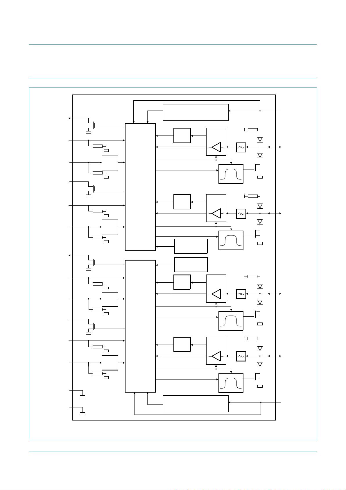
The TJA1024 is a quad LIN transceiver that provides the interface between a Local
Interconnect Network (LIN) master/slave protocol controller and the physical bus in a LIN
network. It comprises two independent and separated dual LIN transceiver blocks on a
single die (only the ground pins GND1 and GND2 are connected internally) with dedicated
supply pins (V
BAT1
for LIN 1/LIN2 and V
BAT2
for LIN3/LIN4).
The TJA1024 is primarily intended for in-vehicle subnetworks using baud rates up to
20 kBd and is compliant with LIN 2.0, LIN 2.1, LIN 2.2, LIN 2.2A and SAE J2602. The
TJA1024 is software compatible with the TJA1022, TJA1027 and TJA1029.
The transmit data streams generated by the protocol controller are converted by the
TJA1024 into optimized bus signals shaped to minimize ElectroMagnetic Emissions
(EME). The LIN bus output pins are pulled HIGH via internal termination resistors. For a
master application, an external resistor in series with a diode should be connected
between pin V
BATx
and the respective LIN pins. The receivers detect receive data streams
on the LIN bus input pins and transfer them via pins RXDx to the microcontroller.
Power consumption is very low when all four transceivers are in Sleep mode. However,
the TJA1024 can still be woken up via pins LINx and SLPx_N.
2. Features and benefits
2.1 General
Four LIN transceivers in a single package
LIN 2.0, LIN 2.1, LIN 2.2, LIN 2.2A and SAE J2602 compliant
Baud rate up to 20 kBd
Very low EME
Very low current consumption in Sleep mode with remote LIN wake-up
Input levels compatible with 3.3 V and 5 V devices
Integrated termination resistors for LIN slave applications
Passive behavior in unpowered state
Operational during cranking pulse: full operation from 5 V upwards
Undervoltage detection
K-line compatible
Leadless DHVQFN24 package (3.5 mm 5.5 mm) with improved Automated Optical
Inspection (AOI)
Dark green product (halogen free and Restriction of Hazardous Substances (RoHS)
compliant)
Software-compatible with the TJA1022, TJA1027 and TJA1029
TJA1024
Quad LIN 2.2A/SAE J2602 transceiver
Rev. 1 — 12 February 2015 Product data sheet
TJA1024 All information provided in this document is subject to legal disclaimers. © NXP Semiconductors N.V. 2015. All rights reserved.
Product data sheet Rev. 1 — 12 February 2015 2 of 25
NXP Semiconductors
TJA1024
Quad LIN 2.2A/SAE J2602 transceiver
2.2 Protection
Very high ElectroMagnetic Immunity (EMI)
Very high ESD robustness: 8 kV according to IEC 61000-4-2 for pins LINx and V
BATx
Bus terminal and battery pins protected against transients in the automotive
environment (ISO 7637)
Bus terminal short-circuit proof to battery and ground
Thermally protected
Initial TXD dominant check when switching to Normal mode
TXD dominant time-out function
3. Quick reference data
4. Ordering information
Table 1. Quick reference data
Symbol Parameter Conditions Min Typ Max Unit
V
BAT
battery supply voltage pins V
BAT1
and V
BAT2
; limiting values 0.3 - +42 V
operating range 5 - 18 V
I
BAT
battery supply current per pin (V
BAT1
or V
BAT2
):
Sleep mode (both channels); bus recessive
(both channels); V
LINx
=V
BATx
; V
SLPx_N
=0V
2.5 7 10 A
Standby mode (both channels); bus recessive
(both channels); V
LINx
=V
BATx
; V
SLPx_N
=0V
2.5 7 10 A
Normal mode (both channels); bus recessive
(both channels); V
TXDx
=5 V; V
LINx
= V
BATx
;
V
SLPx_N
=5 V
300 1600 3200 A
V
LIN
voltage on pin LIN pins LIN1, LIN2, LIN3 and LIN4; limiting value;
with respect to GND and V
BAT
42 - +42 V
V
ESD
electrostatic discharge voltage on pins LIN1, LIN2, LIN3, LIN4, V
BAT1
and V
BAT2
;
according to IEC 61000-4-2
8- +8kV
T
vj
virtual junction temperature 40 - +150 C
Table 2. Ordering information
Type number Package
Name Description Version
TJA1024HG DHVQFN24 plastic dual in-line compatible thermal enhanced very thin quad flat
package; no leads; 24 terminals; body 3.5 5.5 0.85 mm
SOT815-1
TJA1024 All information provided in this document is subject to legal disclaimers. © NXP Semiconductors N.V. 2015. All rights reserved.
Product data sheet Rev. 1 — 12 February 2015 3 of 25
NXP Semiconductors
TJA1024
Quad LIN 2.2A/SAE J2602 transceiver
5. Block diagram
Fig 1. Block diagram
32:(5215(6(7$1'
81'(592/7$*('(7(&7,21
7-$
DDD
&21752/
*1'
%86
7,0(5
9
%$7
/,1
5;'
5;'
7(03(5$785(
3527(&7,21
%86
7,0(5
9
%$7
/,1
6/3B1
7;'
'20
7,0(5
6/3B1
7;'
'20
7,0(5
5;'
5;'
6/3B1
7;'
'20
7,0(5
6/3B1
7;'
'20
7,0(5
%86
7,0(5
/,1
9
%$7
%86
7,0(5
/,1
9
%$7
*1'
32:(5215(6(7$1'
81'(592/7$*('(7(&7,21
9
%$7
9
%$7
7(03(5$785(
3527(&7,21
&21752/
TJA1024 All information provided in this document is subject to legal disclaimers. © NXP Semiconductors N.V. 2015. All rights reserved.
Product data sheet Rev. 1 — 12 February 2015 4 of 25
NXP Semiconductors
TJA1024
Quad LIN 2.2A/SAE J2602 transceiver
6. Pinning information
6.1 Pinning
6.2 Pin description
Fig 2. Pin configuration diagram
DDD
7-$+*
7UDQVSDUHQWWRSYLHZ
*1'
5;'
6/3B1
/,1
7;' 9
%$7
6/3B1 /,1
5;' QF
7;'
*1'
6/3B1 /,1
5;' 9
%$7
7;' /,1
6/3B1 QF
7;'
QF
5
;'
Q
Q
WHUPLQDO
LQGH[DUHD
Table 3. Pin description
Symbol Pin Description
RXD1 1 receive data output 1 (open-drain); active LOW after a wake-up event
SLP1_N 2 sleep control input 1 (active LOW); resets wake-up request on RXD1
TXD1 3 transmit data input 1
RXD2 4 receive data output 2 (open-drain); active LOW after a wake-up event
SLP2_N 5 sleep control input 2 (active LOW); resets wake-up request on RXD2
TXD2 6 transmit data input 2
RXD3 7 receive data output 3 (open-drain); active LOW after a wake-up event
SLP3_N 8 sleep control input 3 (active LOW); resets wake-up request on RXD2
TXD3 9 transmit data input 3
RXD4 10 receive data output 4 (open-drain); active LOW after a wake-up event
SLP4_N 11 sleep control input 4 (active LOW); resets wake-up request on RXD2
TXD4 12 transmit data input 4
n.c. 13 not connected
GND2
[1]
14 ground connection for LIN3 and LIN4
LIN4 15 LIN bus line 4 input/output
V
BAT2
16 battery supply for LIN3 and LIN4
LIN3 17 LIN bus line 3 input/output
n.c. 18 not connected
TJA1024 All information provided in this document is subject to legal disclaimers. © NXP Semiconductors N.V. 2015. All rights reserved.
Product data sheet Rev. 1 — 12 February 2015 5 of 25
NXP Semiconductors
TJA1024
Quad LIN 2.2A/SAE J2602 transceiver
[1] For enhanced thermal and electrical performance, the exposed center pad of the DHVQFN24 package
should be soldered to board ground (and not to any other voltage level).
GND1
[1]
19 ground connection for LIN1 and LIN2
LIN2 20 LIN bus line 2 input/output
V
BAT1
21 battery supply for LIN1 and LIN2
LIN1 22 LIN bus line 1 input/output
n.c. 23 not connected
n.c. 24 not connected
Table 3. Pin description
…continued
Symbol Pin Description
剩余24页未读,继续阅读
资源评论
Autosar汽车电子进阶
- 粉丝: 1w+
- 资源: 8
上传资源 快速赚钱
- 我的内容管理 展开
- 我的资源 快来上传第一个资源
- 我的收益 登录查看自己的收益
- 我的积分 登录查看自己的积分
- 我的C币 登录后查看C币余额
- 我的收藏
- 我的下载
- 下载帮助
安全验证
文档复制为VIP权益,开通VIP直接复制
信息提交成功