没有合适的资源?快使用搜索试试~ 我知道了~
TJA1057.PDF
需积分: 31 15 下载量 17 浏览量
2021-05-27
19:45:51
上传
评论
收藏 376KB PDF 举报
温馨提示
试读
25页
TJA1057.PDF手册
资源详情
资源评论
资源推荐
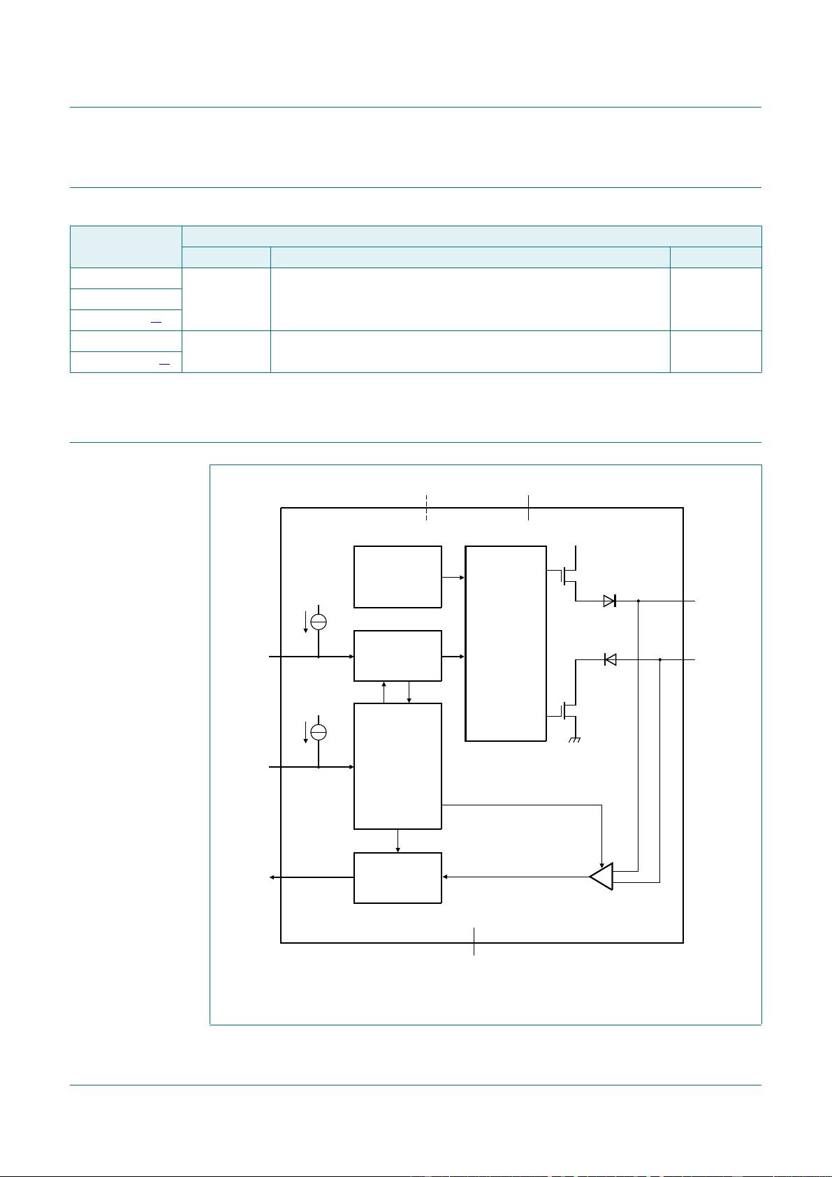
1. General description
The TJA1057 is part of the Mantis family of high-speed CAN transceivers. It provides an
interface between a Controller Area Network (CAN) protocol controller and the physical
two-wire CAN bus. The transceiver is designed for high-speed CAN applications in the
automotive industry, providing the differential transmit and receive capability to (a
microcontroller with) a CAN protocol controller.
The TJA1057 offers a feature set optimized for 12 V automotive applications, with
significant improvements over first- and second-generation CAN transceivers from NXP,
such as the TJA1050, and excellent ElectroMagnetic Compatibility (EMC) performance.
The TJA1057 also displays ideal passive behavior to the CAN bus when the supply
voltage is off.
A V
IO
pin on the TJA1057GT(K)/3 variants allows for direct interfacing with 3.3 V and
5 V-supplied microcontrollers.
The TJA1057 implements the CAN physical layer as defined in the current
ISO11898-2:2003 standard and the pending updated version of ISO11898-2:2016. The
TJA1057T variant is specified for data rates up to 1 Mbit/s. Pending the release of
ISO11898-2:2016 including CAN FD and SAE-J2284-4/5, additional timing parameters
are specified for the TJA1057GT(/3) and TJA1057GTK(/3) variants. This implementation
enables reliable communication in the CAN FD fast phase at data rates up to 5 Mbit/s.
These features make the TJA1057 an excellent choice for HS-CAN networks that only
require basic CAN functionality.
2. Features and benefits
2.1 General
Fully ISO 11898-2:2003 compliant
Optimized for use in 12 V automotive systems
EMC performance satisfies 'Hardware Requirements for LIN, CAN and FlexRay
Interfaces in Automotive Applications’, Version 1.3, May 2012.
V
IO
option allows for direct interfacing with 3.3 V and 5 V-supplied microcontrollers
Non-V
IO
variants can interface with 3.3 V and 5 V-supplied microcontrollers, provided
the microcontroller I/Os are 5 V tolerant.
AEC-Q100 qualified
Dark green product (halogen free and Restriction of Hazardous Substances (RoHS)
compliant)
Available in SO8 package and leadless HVSON8 package (3.0 mm 3.0 mm) with
improved Automated Optical Inspection (AOI) capability
TJA1057
High-speed CAN transceiver
Rev. 5 — 23 May 2016 Product data sheet
有VIO的,支持3.3v和5v的MCU,MCU的TXD和RXD电平由VIO决定;
没有VIO的支持3.3v和5v的MCU,要求MCU的TXD和RXD电平为5V。
TJA1057 All information provided in this document is subject to legal disclaimers. © NXP Semiconductors N.V. 2016. All rights reserved.
Product data sheet Rev. 5 — 23 May 2016 2 of 25
NXP Semiconductors
TJA1057
High-speed CAN transceiver
2.2 Predictable and fail-safe behavior
Functional behavior predictable under all supply conditions
Transceiver disengages from bus when not powered (zero load)
Transmit Data (TXD) dominant time-out function
Internal biasing of TXD and S input pins
2.3 Protection
High ESD handling capability on the bus pins (8 kV IEC and HBM)
Bus pins protected against transients in automotive environments
Undervoltage detection on pins V
CC
and V
IO
Thermally protected
2.4 TJA1057GT(/3)/TJA1057GTK(/3)
Timing guaranteed for data rates up to 5 Mbit/s
Improved TXD to RXD propagation delay of 210 ns
3. Quick reference data
Table 1. Quick reference data
Symbol Parameter Conditions Min Typ Max Unit
V
CC
supply voltage 4.75 - 5.25 V
V
IO
supply voltage on pin V
IO
2.95 - 5.25 V
V
uvd(VCC)
undervoltage detection voltage
on pin V
CC
3.5 4 4.3 V
V
uvd(VIO)
undervoltage detection voltage
on pin V
IO
2.1 - 2.8 V
I
CC
supply current Silent mode 0.1 - 1.2 mA
Normal mode; bus recessive 2 5 10 mA
Normal mode; bus dominant 20 45 70 mA
I
IO
supply current on pin V
IO
Silent mode - 3 16 A
Normal mode
recessive; V
TXD
=V
IO
-730A
dominant; V
TXD
= 0 V - 110 320 A
V
ESD
electrostatic discharge voltage IEC 61000-4-2 at pins CANH and CANL 8- +8 kV
V
CANH
voltage on pin CANH limiting value according to IEC60134 42 - +42 V
V
CANL
voltage on pin CANL limiting value according to IEC60134 42 - +42 V
T
vj
virtual junction temperature 40 - +150 C
TJA1057 All information provided in this document is subject to legal disclaimers. © NXP Semiconductors N.V. 2016. All rights reserved.
Product data sheet Rev. 5 — 23 May 2016 3 of 25
NXP Semiconductors
TJA1057
High-speed CAN transceiver
4. Ordering information
[1] TJA1057GT/3 and TJA1057GTK/3 variants have a V
IO
pin.
5. Block diagram
Table 2. Ordering information
Type number Package
Name Description Version
TJA1057T SO8 plastic small outline package; 8 leads; body width 3.9 mm SOT96-1
TJA1057GT
TJA1057GT/3
[1]
TJA1057GTK HVSON8 plastic thermal enhanced very thin small outline package; no leads;
8 terminals; body 3 3 0.85 mm
SOT782-1
TJA1057GTK/3
[1]
(1) V
IO
=V
CC
in non-V
IO
product variants TJA1057(G)T(K)
Fig 1. Block diagram
7(03(5$785(
3527(&7,21
7,0(287
02'(
&21752/
7;'
5;'
6/23(
&21752/
$1'
'5,9(5
9
&&
&$1+
&$1/
*1'
7-$
6
DDD
'5,9(5
9
,2
9
,2
9
&&
9
,2
TJA1057 All information provided in this document is subject to legal disclaimers. © NXP Semiconductors N.V. 2016. All rights reserved.
Product data sheet Rev. 5 — 23 May 2016 4 of 25
NXP Semiconductors
TJA1057
High-speed CAN transceiver
6. Pinning information
6.1 Pinning
6.2 Pin description
[1] HVSON8 package die supply ground is connected to both the GND pin and the exposed center pad. The
GND pin must be soldered to board ground. For enhanced thermal and electrical performance, it is
recommended that the exposed center pad also be soldered to board ground.
a. SO8 b. SO8 with V
IO
c. HVSON8 d. HVSON8 with V
IO
Fig 2. Pin configuration diagrams
7-$7
7-$*7
7;'
6
*1' &$1+
9
&&
&$1/
5;' QF
DDD
7-$*7
7;'
6
*1' &$1+
9
&&
&$1/
5;'
9
,
2
DDD
5;'
9
&&
*1'
7;'
QF
&$1/
&$1+
6
DDD
7-$*7.
WHUPLQDO
LQGH[DUHD
7UDQVSDUHQWWRSYLHZ
5;'
9
&&
*1'
7;'
9
,
2
&$1/
&$1+
6
DDD
7-$*7.
WHUPLQDO
LQGH[DUHD
7UDQVSDUHQWWRSYLHZ
Table 3. Pin description
Symbol Pin Description
TXD 1 transmit data input
GND
[1]
2 ground
V
CC
3 supply voltage
RXD 4 receive data output; reads out data from the bus lines
n.c. 5 not connected in TJA1057T, TJA1057GT and TJA1057GTK
V
IO
5 supply voltage for I/O level adapter in TJA1057GT/3 and TJA1057GTK/3
CANL 6 LOW-level CAN bus line
CANH 7 HIGH-level CAN bus line
S 8 Silent mode control input
TJA1057 All information provided in this document is subject to legal disclaimers. © NXP Semiconductors N.V. 2016. All rights reserved.
Product data sheet Rev. 5 — 23 May 2016 5 of 25
NXP Semiconductors
TJA1057
High-speed CAN transceiver
7. Functional description
7.1 Operating modes
The TJA1057 supports two operating modes, Normal and Silent. The operating mode is
selected via pin S. See Table 4
for a description of the operating modes under normal
supply conditions.
[1] ‘x’ = don’t care.
7.1.1 Normal mode
A LOW level on pin S selects Normal mode. In this mode, the transceiver can transmit and
receive data via the bus lines, CANH and CANL (see Figure 1
for the block diagram). The
differential receiver converts the analog data on the bus lines into digital data which is
output on pin RXD. The slopes of the output signals on the bus lines are controlled
internally and are optimized in a way that guarantees the lowest possible EME.
7.1.2 Silent mode
A HIGH level on pin S selects Silent mode. The transmitter is disabled in Silent mode,
releasing the bus pins to recessive state. All other IC functions, including the receiver,
continue to operate as in Normal mode. Silent mode can be used to prevent a faulty CAN
controller disrupting all network communications.
7.2 Fail-safe features
7.2.1 TXD dominant time-out function
A 'TXD dominant time-out' timer is started when pin TXD is set LOW. If the LOW state on
this pin persists for longer than t
to(dom)TXD
, the transmitter is disabled, releasing the bus
lines to recessive state. This function prevents a hardware and/or software application
failure from driving the bus lines to a permanent dominant state (blocking all network
communications). The TXD dominant time-out timer is reset when pin TXD is set HIGH.
The TXD dominant time-out time also defines the minimum possible bit rate of
approximately 25 kbit/s.
7.2.2 Internal biasing of TXD and S input pins
Pins TXD and S have internal pull-ups to V
CC
(or V
IO
in TJA1057GT(K)/3 variants) to
ensure a safe, defined state in case one or both of these pins are left floating. Pull-up
currents flow in these pins in all states; both pins should be held HIGH in Silent mode to
minimize supply current.
Table 4. Operating modes
Mode Inputs Outputs
Pin S Pin TXD CAN driver Pin RXD
Normal LOW LOW dominant LOW
HIGH recessive LOW when bus dominant
HIGH when bus recessive
Silent HIGH x
[1]
biased to recessive LOW when bus dominant
HIGH when bus recessive
剩余24页未读,继续阅读
ablitt_Smart_home
- 粉丝: 1
- 资源: 32
上传资源 快速赚钱
- 我的内容管理 展开
- 我的资源 快来上传第一个资源
- 我的收益 登录查看自己的收益
- 我的积分 登录查看自己的积分
- 我的C币 登录后查看C币余额
- 我的收藏
- 我的下载
- 下载帮助
安全验证
文档复制为VIP权益,开通VIP直接复制
信息提交成功
评论0