ADSemiconductor
®
TS20 (20-CH Auto Sensitivity Calibration Capacitive Touch Sensor)
AD Semiconductor Confidential 4 / 46
Content
GENERAL ................................................................................................................................. 2
REVISION HISTORY............................................................................................................... 3
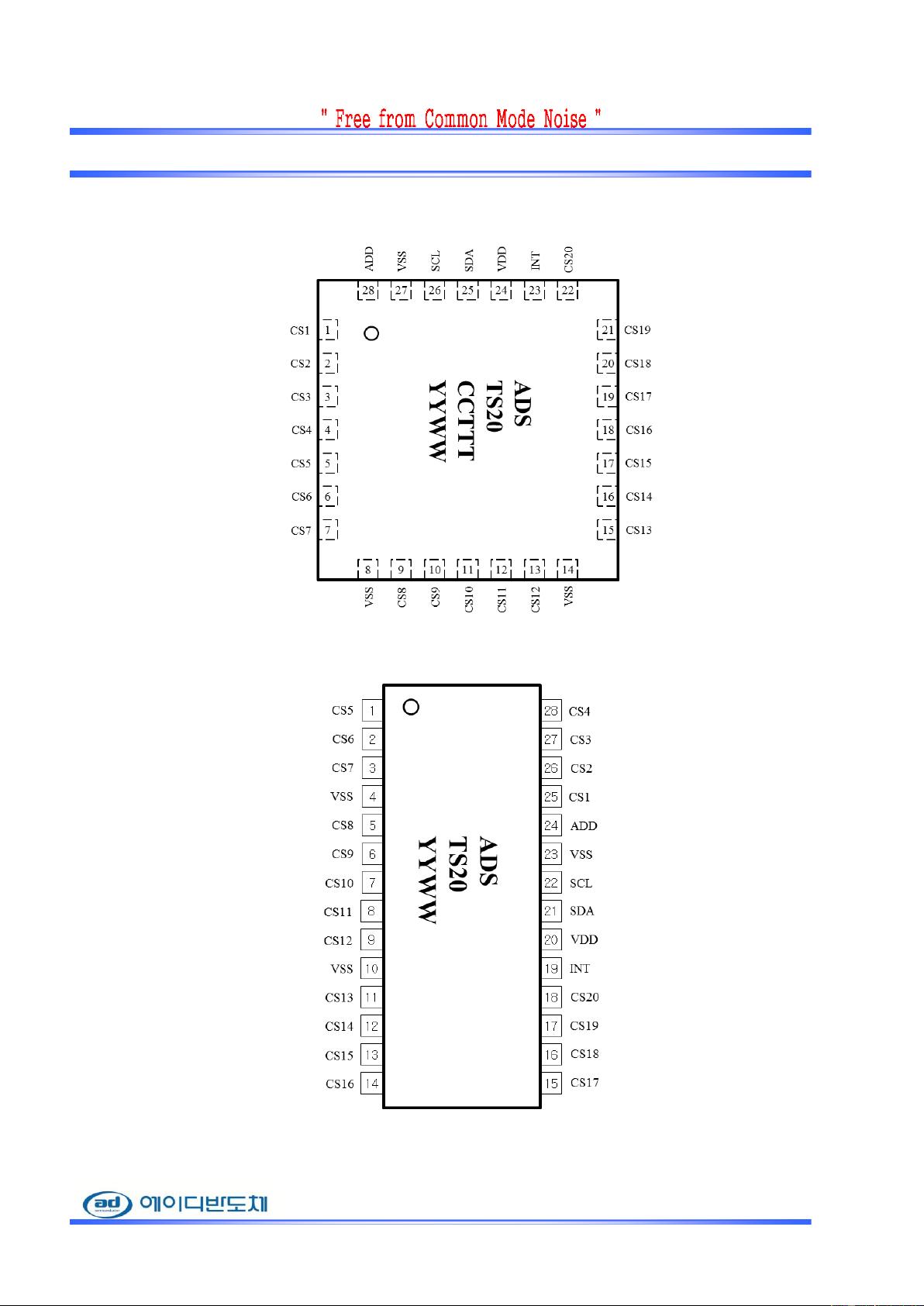
1 PIN CONFIGURATION ................................................................................................... 6
2 PIN DESCRIPTION .......................................................................................................... 7
2.1 TS20-Q (28QFN PACKAGE) ....................................................................................... 8
2.2 TS20 (28TSSOP PACKAGE) ...................................................................................... 10
3 ABSOLUTE MAXIMUM RATING ............................................................................... 12
4 ESD & LATCH-UP CHARACTERISTICS .................................................................... 12
4.1 ESD CHARACTERISTICS ............................................................................................ 12
4.2 LATCH-UP CHARACTERISTICS ................................................................................... 12
5 ELECTRICAL CHARACTERISTICS ............................................................................ 13
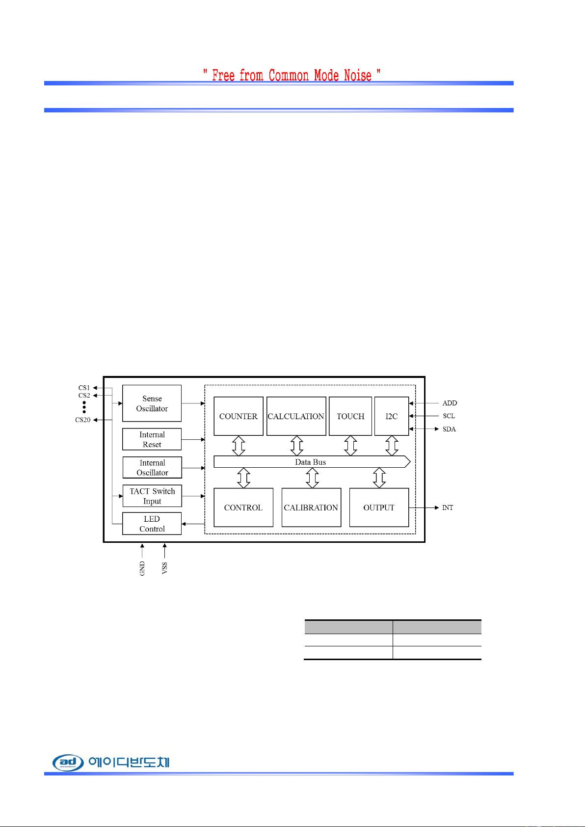
6 TS20 IMPLEMENTATION ............................................................................................ 14
6.1 CS IMPLEMENTATION ................................................................................................ 14
6.2 CS IMPLEMENTATION FOR TACT SWITCH INPUT ........................................................ 15
6.3 CS IMPLEMENTATION FOR LED DRIVE OUTPUT ........................................................ 15
6.4 INTERNAL RESET OPERATION .................................................................................... 16
6.5 POWER ON SEQUENCE FOR SCL & SDA.................................................................... 16
7 I2C INTERFACE............................................................................................................. 17
7.1 I2C ENABLE / DISABLE ............................................................................................. 17
7.2 START & STOP CONDITION ....................................................................................... 17
7.3 DATA VALIDITY ........................................................................................................ 17
7.4 BYTE FORMAT .......................................................................................................... 17
7.5 ACKNOWLEDGE ........................................................................................................ 18
7.6 FIRST BYTE ............................................................................................................... 18
7.6.1 Slave Address....................................................................................................... 18
7.6.2 R/W
─
...................................................................................................................... 18
7.7 TRANSFERRING DATA ............................................................................................... 19
7.7.1 Write Operation ................................................................................................... 19
7.7.2 Read Operation .................................................................................................... 19
7.7.3 Read/Write Operation .......................................................................................... 19
7.8 I2C WRITE AND READ OPERATIONS IN NORMAL MODE .............................................. 20
8 TS20 CONTROL REGISTER LIST ............................................................................... 21
8.1 I2C REGISTER MAP ................................................................................................... 21
8.2 DETAILS .................................................................................................................... 23
8.2.1 Sensitivity Control Register ................................................................................. 23
8.2.2 General Control Register 1 .................................................................................. 24
8.2.3 General Control Register 2 .................................................................................. 25