没有合适的资源?快使用搜索试试~ 我知道了~
txs0108e-数据手册.pdf
资源详情
资源评论
资源推荐
A1
A2
Data
A3
A4
A5
A6
A7
A8
GND
OE
V
CCA
V
CCB
1.8-V
System
Controller
B1
B2
B3
B4
B5
B6
B7
B8
TXS0108E
3.3-V
System
Controller
0.1 PF
3.3 V
0.1 PF
1.8 V
Product
Folder
Order
Now
Technical
Documents
Tools &
Software
Support &
Community
本文档旨在为方便起见,提供有关 TI 产品中文版本的信息,以确认产品的概要。 有关适用的官方英文版本的最新信息,请访问 www.ti.com,其内容始终优先。 TI 不保证翻译的准确
性和有效性。 在实际设计之前,请务必参考最新版本的英文版本。
English Data Sheet: SCES642
TXS0108E
ZHCSE13F –DECEMBER 2007–REVISED JANUARY 2019
TXS0108E面面向向开开漏漏和和推推挽挽应应用用的的
8 位位双双向向电电压压电电平平转转换换 应应用用
1
1 特特性性
1
• 无需方向控制信号
• 最大数据速率
– 110Mbps(推挽)
– 1.2Mbps(开漏)
• A 端口 1.2V 至 3.6V;B 端口 1.65V 至 5.5V (V
CCA
≤ V
CCB
)
• 无需电源定序 - V
CCA
或 V
CCB
均可优先斜升
• 锁断性能超过 100mA,符合
JESD 78 II 类规范的要求
• 静电放电 (ESD) 保护性能超过 JESD 22 规范的要
求(A 端口)
– 2000V 人体放电模型 (A114-B)
– 150V 机器模型 (A115-A)
– 1000V 充电器件模型 (C101)
• IEC 61000-4-2 ESD(B 端口)
– ±8kV 接触放电
– ±6kV 气隙放电
2 应应用用
• 手持终端
• 智能电话
• 平板电脑
• 台式计算机
3 说说明明
这款 8 位非反向转换器使用两个独立的可配置电源
轨。A 端口跟踪 V
CCA
引脚的电源电压。V
CCA
引脚可
接受 1.2V 到 3.6V 范围内的任意电源电压。B 端口跟
踪 V
CCB
引脚的电源电压。V
CCB
引脚可接受 1.65V 到
5.5V 范围内的任意电源电压。这两个输入电源引脚可
实现 1.2V、1.8V、2.5V、3.3V 和 5V 电压节点之间的
任意低压双向转换。
输出使能 (OE) 输入为低电平时,所有输出均将置于高
阻抗 (Hi-Z) 状态。
为确保输出在上电或断电期间处于 Hi-Z 状态,需通过
一个下拉电阻将 OE 接至 GND。该电阻的最小值取决
于驱动器的拉电流能力。
器器件件信信息息
(1)
器器件件型型号号 封封装装 封封装装尺尺寸寸((标标称称值值))
TXS0108EPW TSSOP (20) 6.50mm x 6.40mm
TXS0108ERGY VQFN (20) 4.50mm x 3.50mm
TXS0108EZXY UFBGA (20) 3.00mm x 2.50mm
(1) 如需了解所有可用封装,请参阅数据表末尾的可订购产品附
录。
简简化化应应用用
2
TXS0108E
ZHCSE13F –DECEMBER 2007–REVISED JANUARY 2019
www.ti.com.cn
Copyright © 2007–2019, Texas Instruments Incorporated
目目录录
1 特特性性.......................................................................... 1
2 应应用用.......................................................................... 1
3 说说明明.......................................................................... 1
4 修修订订历历史史记记录录 ........................................................... 2
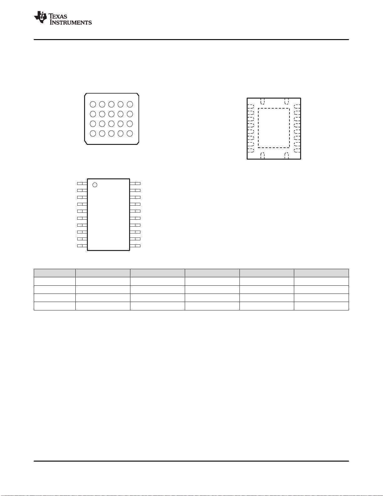
5 Pin Configuration and Functions......................... 3
6 Specifications......................................................... 5
6.1 Absolute Maximum Ratings ..................................... 5
6.2 ESD Ratings.............................................................. 5
6.3 Recommended Operating Conditions ...................... 6
6.4 Thermal Information.................................................. 6
6.5 Electrical Characteristics: T
A
= –40°C to 85°C ........ 7
6.6 Timing Requirements: V
CCA
= 1.2 V ........................ 8
6.7 Timing Requirements: V
CCA
= 1.5 V ± 0.1 V ............ 8
6.8 Timing Requirements: V
CCA
= 1.8 V ± 0.15 V .......... 8
6.9 Timing Requirements: V
CCA
= 2.5 V ± 0.2 V ............ 8
6.10 Timing Requirements: V
CCA
= 3.3 V ± 0.3 V .......... 8
6.11 Switching Characteristics: V
CCA
= 1.2 V................. 9
6.12 Switching Characteristics: V
CCA
= 1.5 V ± 0.1 V .. 10
6.13 Switching Characteristics: V
CCA
= 1.8 V ± 0.15 V 11
6.14 Switching Characteristics: V
CCA
= 2.5 V ± 0.2 V .. 12
6.15 Switching Characteristics: V
CCA
= 3.3 V ± 0.3 V .. 13
6.16 Operating Characteristics: V
CCA
= 1.2 V to 1.5 V,
V
CCB
= 1.2V to 1.5 V................................................ 14
6.17 Operating Characteristics: V
CCA
= 1.8 V to 3.3 V,
V
CCB
= 1.8 V to 3.3 V............................................... 14
7 Typical Characteristics........................................ 15
8 Parameter Measurement Information ................ 16
8.1 Load Circuits ........................................................... 16
8.2 Voltage Waveforms................................................. 17
9 Detailed Description............................................ 18
9.1 Overview ................................................................. 18
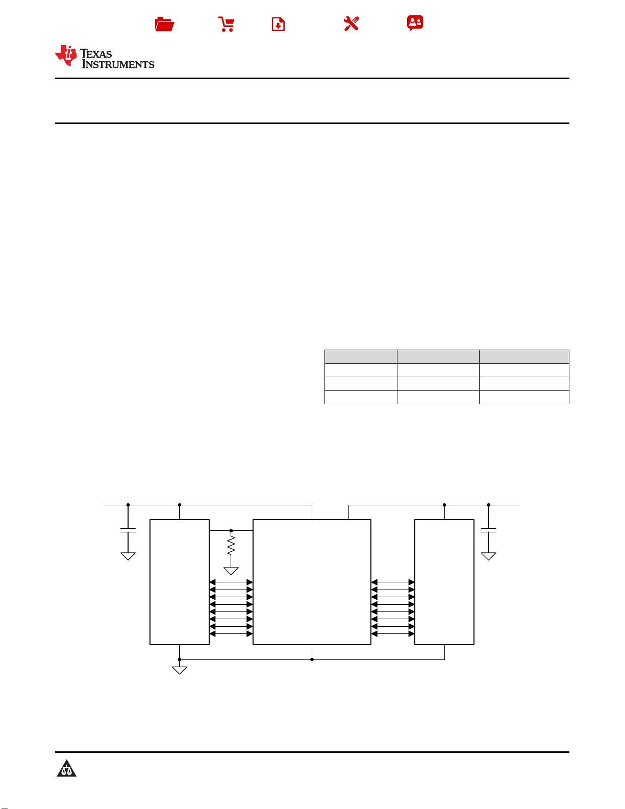
9.2 Functional Block Diagram ....................................... 18
9.3 Feature Description................................................. 19
9.4 Device Functional Modes........................................ 20
10 Application and Implementation........................ 21
10.1 Application Information.......................................... 21
10.2 Typical Application ............................................... 21
11 Power Supply Recommendations ..................... 23
12 Layout................................................................... 23
12.1 Layout Guidelines ................................................. 23
12.2 Layout Example .................................................... 23
13 器器件件和和文文档档支支持持 ..................................................... 24
13.1 社区资源................................................................ 24
13.2 商标 ....................................................................... 24
13.3 静电放电警告......................................................... 24
13.4 术语表 ................................................................... 24
14 机机械械、、封封装装和和可可订订购购信信息息....................................... 24
4 修修订订历历史史记记录录
Changes from Revision E (February 2018) to Revision F Page
• Changed T
A
from 125°C to 85°C in the Recommended Operating Conditions table............................................................. 6
Changes from Revision D (February 2016) to Revision E Page
• Added junction temperature .................................................................................................................................................. 5
Changes from Revision C (December 2014) to Revision D Page
• 已更改 ESD
额定值表,
......................................................................................................................................................... 1
Changes from Revision B (November 2013) to Revision C Page
• 已添加
引脚配置和功能
部分,ESD
额定值
表,
特性 说明
部分、
器件功能模式
、
应用和实施
部分、
电源建议
部分、
布局
部分、
器件和文档支持
部分以及
机械、封装和可订购信息
部分 .................................................................................... 1
19
18
17
16
15
14
12
13
1
2
3
4
5
6
7
9
8
10 11
20
B1
B2
B4
B6
B8
VCCB
B3
B5
B7
A1
A2
A4
A6
A8
VCCA
A3
A5
A7
OE GND
19
18
17
16
15
14
12
13
1
2
3
4
5
6
7
9
8
10 11
20
A1
B1
A2
A4
A6
A8
VCCA
A3
A5
A7
B2
B4
B6
B8
VCCB
B3
B5
B7
OE
GND
Exposed
Center
Pad
A
B
C
D
21 3 4 5
3
TXS0108E
www.ti.com.cn
ZHCSE13F –DECEMBER 2007–REVISED JANUARY 2019
Copyright © 2007–2019, Texas Instruments Incorporated
5 Pin Configuration and Functions
ZXY PACKAGE
20 BUMP
(BOTTOM VIEW)
PW PACKAGE
20-PIN TSSOP
(TOP VIEW)
RGY PACKAGE
20 PINS
(TOP VIEW)
The exposed center pad, if used, must be
connected as a secondary ground or left
electrically open.
Table 1. Pin Assignments
1 2 3 4 5
D VCCB B2 B4 B6 B8
C B1 B3 B5 B7 GND
B A1 A3 A5 A7 OE
A VCCA A2 A4 A6 A8
4
TXS0108E
ZHCSE13F –DECEMBER 2007–REVISED JANUARY 2019
www.ti.com.cn
Copyright © 2007–2019, Texas Instruments Incorporated
(1) I = input, O = output, I/O = input and output, P = power
Pin Functions
PIN NO.
TYPE
(1)
DESCRIPTION
NAME PW, RGY ZXY
A1 1 B1 I/O Input/output 1. Referenced to V
CCA
A2 3 A2 I/O Input/output 2. Referenced to V
CCA
A3 4 B2 I/O Input/output 3. Referenced to V
CCA
A4 5 A3 I/O Input/output 4. Referenced to V
CCA
A5 6 B3 I/O Input/output 5. Referenced to V
CCA
A6 7 A4 I/O Input/output 6. Referenced to V
CCA
A7 8 B4 I/O Input/output 7. Referenced to V
CCA
A8 9 A5 I/O Input/output 8. Referenced to V
CCA
B1 20 C 1 I/O Input/output 1. Referenced to V
CCB
B2 18 D2 I/O Input/output 2. Referenced to V
CCB
B3 17 C2 I/O Input/output 3. Referenced to V
CCB
B4 16 D3 I/O Input/output 4. Referenced to V
CCB
B5 15 C3 I/O Input/output 5. Referenced to V
CCB
B6 14 D4 I/O Input/output 6. Referenced to V
CCB
B7 13 C4 I/O Input/output 7. Referenced to V
CCB
B8 12 D5 I/O Input/output 8. Referenced to V
CCB
GND 11 C5 — Ground
OE 10 B5 I
Tri-state output-mode enable. Pull OE low to place all outputs in 3-state mode.
Referenced to V
CCA
.
VCCA 2 A1 P A-port supply voltage. 1.2 V ≤ V
CCA
≤ 3.6 V, V
CCA
≤ V
CCB
.
VCCB 19 D1 P B-port supply voltage. 1.65 V ≤ V
CCB
≤ 5.5 V.
Thermal Pad —
For the RGY package, the exposed center thermal pad must be either be connected to
Ground or left electrically opened.
5
TXS0108E
www.ti.com.cn
ZHCSE13F –DECEMBER 2007–REVISED JANUARY 2019
Copyright © 2007–2019, Texas Instruments Incorporated
(1) Stresses beyond those listed under Absolute Maximum Ratings may cause permanent damage to the device. These are stress ratings
only, and functional operation of the device at these or any other conditions beyond those indicated under Recommended Operating
Conditions is not implied. Exposure to absolute-maximum-rated conditions for extended periods may affect device reliability.
(2) The input and output negative Voltage ratings may be exceeded if the input and output current ratings are observed.
(3) The value of V
CCA
and V
CCB
are provided in the recommended operating conditions table.
6 Specifications
6.1 Absolute Maximum Ratings
(1)
over operating free-air temperature range (unless otherwise noted)
MIN MAX UNIT
Supply voltage, V
CCA
–0.5 4.6 V
Supply voltage, V
CCB
–0.5 5.5 V
Input voltage, V
I
(2)
A port –0.5 4.6
V
B port –0.5 6.5
Voltage applied to any output
in the high-impedance or power-off state, V
O
(2)
A port –0.5 4.6
V
B port –0.5 6.5
Voltage applied to any output in the high or low state, V
O
(2) (3)
A port –0.5 V
CCA
+ 0.5 V
B port –0.5 V
CCB
+ 0.5 V
Input clamp current, I
IK
V
I
< 0 –50 mA
Output clamp current, I
OK
V
O
< 0 –50 mA
Continuous output current, I
O
–50 50 mA
Continuous current through V
CCA
, V
CCB
, or GND –100 100 mA
Junction temperature, T
J
150 °C
Storage temperature, T
stg
–65 150 °C
(1) JEDEC document JEP155 states that 500 V HBM allows safe manufacturing with a standard ESD control process.
(2) JEDEC document JEP157 states that 250 V CDM allows safe manufacturing with a standard ESD control process.
6.2 ESD Ratings
VALUE UNIT
V
(ESD)
Electrostatic
discharge
Human body model (HBM), per ANSI/ESDA/JEDEC JS-001
(1)
±2000
V
Charged-device model (CDM), per JEDEC specification JESD22-C101
(2)
±1000
Machine model (MM) ±150
IEC 61000-4-2 ESD (B Port) Contact Discharge ±8000
IEC 61000-4-2 ESD (B Port) Air-Gap Discharge ±6000
剩余38页未读,继续阅读
hjx_ty
- 粉丝: 0
- 资源: 4
上传资源 快速赚钱
- 我的内容管理 展开
- 我的资源 快来上传第一个资源
- 我的收益 登录查看自己的收益
- 我的积分 登录查看自己的积分
- 我的C币 登录后查看C币余额
- 我的收藏
- 我的下载
- 下载帮助
安全验证
文档复制为VIP权益,开通VIP直接复制
信息提交成功
评论0