没有合适的资源?快使用搜索试试~ 我知道了~
NXP S32K3xx DataSheet
需积分: 1 9 下载量 81 浏览量
2023-03-20
13:24:53
上传
评论
收藏 1.79MB PDF 举报
温馨提示
试读
141页
Supports S32K344, S32K324, S32K314, S32K312, S32K341 and S32K342. Data is preliminary for S32K311, S32K310, S32K328, S32K338, S32K348, S32K358 and S32K388
资源推荐
资源详情
资源评论
• Operating characteristics
— Voltage range: 2.97 V to 5.5 V
— Ambient temperature range: -40 °C to 125 °C for all
power modes
• Arm
™
Cortex-M7 core, 32-bit CPU
— M7 supports up to 300 MHz frequency with 2.14
DMIPS / MHz
— Arm Core based on the Armv7 and Thumb
®
-2 ISA
— Integrated Digital Signal Processor (DSP)
— Configurable Nested Vectored Interrupt Controller
(NVIC)
— Single Precision Floating Point Unit (FPU)
• Clock interfaces
— 8 - 40 MHz Fast External Oscillator (FXOSC)
— 48 MHz Fast Internal RC oscillator (FIRC)
— 32 kHz Low Power Oscillator (SIRC)
— 32 kHz Slow External Oscillator (SXOSC)
— System Phased Lock Loop (SPLL)
• I/O and package
— LQFP48, MAXQFP100, MAXQFP172,
MAPBGA257, MAPBGA289, MaxQFP172 with
Exposed pad (EP) package options
• Up to 32-channel DMA with up to 128 request sources
using DMAMUX
• Memory and memory interfaces
— Up to 8 MB program flash memory with ECC
— Up to 128 K of flexible program or data flash
memory
— Up to 512 KB SRAM with ECC, includes 192 KB of
TCM RAM ensuring maximum CPU performance of
fast control loops with minimal latency
— Data and instruction cache for each core to
minimize performance impact of memory access
latencies
— QuadSPI support
• Mixed-signal analog
— Up to three 12-bit Analog-to-Digital Converters
(ADC) with up to 24 channel analog inputs per
module
— One Temperature Sensor (TempSense)
— Up to three Analog Comparators (CMP), with each
comparator having an internal 8-bit DAC
• Human-Machine Interface (HMI)
— Up to 235 GPIO pins
— Non-Maskable Interrupt (NMI)
— Up to 60 pins with wakeup capability
— Up to 32 pins with interrupt support
S32K3XX
S32K3xx Data Sheet
Supports S32K344, S32K324, S32K314, S32K312, S32K341 and S32K342.
Data is preliminary for S32K311, S32K310, S32K328, S32K338, S32K348,
S32K358 and S32K388
Rev. 6 — 11/2022
Data Sheet: Technical Data
NXP reserves the right to change the detail specifications as may be required to
permit improvements in the design of its products.
• Power management
— Low-power Arm Cortex-M7 core with excellent
energy efficiency, balanced with performance
— Power Management Controller (PMC) with
simplified mode management (RUN and
STANDBY)
— Supports peripheral specific clock gating. Only
specific peripherals remain working in low power
modes.
• Communications interfaces
— Up to 16 serial communication interface (LPUART)
modules, with LIN, UART and DMA support
— Up to six Low Power Serial Peripheral Interface
(LPSPI) modules with DMA support
— Up to two Low Power Inter-Integrated Circuit
(LPI2C) modules with DMA support
— Up to six FlexCAN modules (with optional CAN-FD
support)
— FlexIO module for flexible and high performance
serial interfaces
— Up to two Ethernet module
— Up to two Synchronous Audio Interface (SAI)
modules
• Reliability, safety and security
— Hardware Security Engine (HSE_B) - Supports AES
accelerator(for K388 only)
— Up to two Internal Software Watchdog Timers
(SWT)
— Error-Correcting Code (ECC) on all memories
— Error Detection Code (EDC) on data path
— Cyclic Redundancy Check (CRC) module
— 120-bit Unique Identification (ID) number
— Extended Cross domain Domain Controller
(XRDC), providing protection for master core
access rights
— Virtualization Wrapper (VIRT_WRAPPER),
providing I/O protection
•
Debug functionality
— Serial Wire JTAG debug Port (SWJ-DP), with 2 pin
Serial Wire Debug (SWD) for external debugger
— Debug Watchpoint and Trace (DWT), with four
configurable comparators as hardware watchpoints
— Serial Wire Output (SWO)-synchronous trace data
support
— Instrumentation Trace Macrocell (ITM) with
software and hardware trace, plus time stamping
— CoreSight AHB Trace Macrocell (HTM)
— Flash Patch and Breakpoints (FPB) with ability to
patch code and data from code space to system
space
— Serial Wire Viewer (SWV): A trace capability
providing displays of reads, writes, exceptions, PC
Samples and print
— Full data trace for up to 16 output wide
— Embedded Cross Trigger (ECT) is used for
multicore run-control and trace cross triggering,
using CoreSight Cross Trigger Interface (CTI)
• Timing and control
— Up to three enhanced modular I/O system (eMIOS),
offering up to 72 timer channels (IC/OC/PWM)
— Up to two System Timer Modules (STM)
— Up to two Logic Control Units (LCU)
— Full cross triggering support for ADC / timer (BCTU)
— One Trigger MUX Control (TRGMUX) module
— Up to three Periodic Interrupt Timer (PIT) modules
— 32-bit Real Time Counter (RTC) with autonomous
periodic interrupt (API) function
NXP Semiconductors
S32K3xx Data Sheet, Rev. 6, 11/2022
Data Sheet: Technical Data Preliminary Information 2 / 141
Contents
1 Overview............................................................ 5
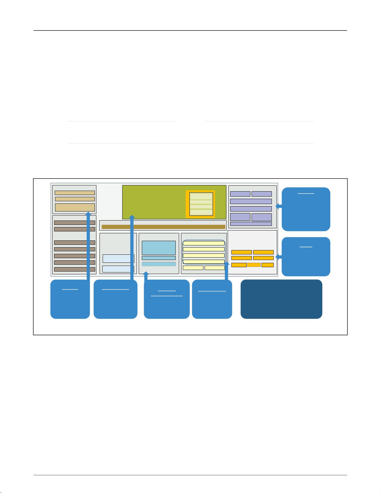
2 Block diagram.....................................................5
3 Feature comparison......................................... 12
4 Ordering information.........................................17
4.1 Determining valid orderable parts ................ 17
5 General.............................................................17
5.1 Absolute maximum ratings............................18
5.2 Voltage and current operating requirements.19
5.3 Thermal operating characteristics.................21
5.4 ESD and Latch-up Protection Characteristics
...................................................................... 22
6 Power management......................................... 22
6.1 Power management system - S32K344,
S32K324, S32K341, S32K314, S32K342, and
S32K322....................................................... 23
6.2 Power management system - S32K312,
S32K311, S32K310...................................... 24
6.3 Power management system - S32K358,
S32K348, S32K338, S32K328......................25
6.4 Power management system - S32K388....... 26
6.5 Power mode transition operating behaviors..26
6.5.1 Power mode transition operating behavior... 26
6.5.2 Boot time, HSE firmware not installed.......... 27
6.5.3 Boot time, HSE firmware installed................ 27
6.5.4 HSE firmware memory verification time
examples.......................................................28
6.6 Supply Monitoring......................................... 32
6.7 Recommended Decoupling Capacitors........ 34
6.8 V15 regulator (SMPS option) electrical
specifications................................................ 46
6.9 V15 regulator (BJT option, NPN ballast
transistor control) electrical specifications.... 47
6.10 V11 regulator (NMOS ballast transistor control)
electrical specifications................................. 48
6.11 Supply currents............................................. 49
6.12 Operating mode............................................ 68
6.13 Cyclic wake-up current .................................70
7 I/O parameters................................................. 70
7.1 GPIO DC electrical specifications, 3.3V Range
(2.97V - 3.63V)..............................................70
7.2 GPIO DC electrical specifications, 5.0V (4.5V -
5.5V)............................................................. 74
7.3 5.0V (4.5V - 5.5V) GPIO Output AC
Specification..................................................78
7.4 3.3V (2.97V - 3.63V) GPIO Output AC
Specification..................................................79
8 Glitch Filter....................................................... 80
9 Flash memory specification..............................81
9.1 Flash memory program and erase
specifications................................................ 81
9.2 Flash memory Array Integrity and Margin Read
specifications................................................ 82
9.3 Flash memory module life specifications...... 83
9.3.1 Data retention vs program/erase cycles....... 83
9.4 Flash memory AC timing specifications........ 84
9.5 Flash memory read timing parameters......... 84
10 Analog modules................................................85
10.1 SAR ADC...................................................... 85
10.2 Supply Diagnosis.......................................... 88
10.3 Low Power Comparator (LPCMP)................ 88
10.4 Temperature Sensor..................................... 92
11 Clocking modules............................................. 93
11.1 FIRC..............................................................93
11.2 SIRC............................................................. 93
11.3 PLL................................................................93
11.4 Fast External Oscillator (FXOSC)................. 95
11.5 Slow Crystal Oscillator (SXOSC).................. 97
12 Communication interfaces................................97
12.1 LPSPI............................................................97
12.1.1 LPSPI............................................................97
12.1.2 LPSPI0 20 MHz and 15 MHz Combinations102
12.2 I
2
C............................................................... 102
12.3 FlexCAN characteristics..............................102
12.4 SAI electrical specifications........................ 102
12.4.1 SAI Electrical Characteristics, Slave Mode.102
12.4.2 SAI Electrical Characteristics, Master Mode104
12.5 Ethernet characteristics.............................. 105
12.5.1 Ethernet MII (100 Mbps)............................. 105
12.5.2 Ethernet MII (200 Mbps)............................. 107
12.5.3 Ethernet RMII..............................................109
12.5.4 Ethernet RGMII........................................... 111
12.5.5 MDIO timing specifications......................... 112
12.6 QuadSPI..................................................... 113
12.6.1 QuadSPI Quad 3.3V SDR 120MHz............ 113
12.6.2 QuadSPI Octal 3.3V DDR 100MHz............ 115
12.6.3 QuadSPI Octal 3.3V DDR 120MHz............ 116
12.7 uSDHC........................................................117
12.7.1 uSDHC SDR electrical specifications......... 117
12.7.2 uSDHC DDR electrical specifications......... 118
12.8 LPUART specifications............................... 120
13 Debug modules.............................................. 120
13.1 Debug trace timing specifications............... 120
13.2 SWD electrical specifications......................121
13.3 JTAG electrical specifications..................... 122
14 Thermal Attributes.......................................... 124
14.1 Description.................................................. 124
14.2 Thermal characteristics...............................125
15 Dimensions.....................................................127
15.1 Obtaining package dimensions...................127
16 Revision history.............................................. 127
1 Overview
The S32K3xx product series further extends the highly-scalable portfolio of Arm
®
Cortex
®
- M0+/M4F S32K1xx chips in the
automotive industry with the Arm Cortex-M7 core at higher frequency, more memory, ASIL-B and D rating and advanced security
module. With a focus on automotive environment robustness, the S32K3xx product series devices are well suited to a wide range
of applications in electrical harsh environments, and are optimized for cost-sensitive applications offering new, space saving
package options. The S32K3xx series offers a broad range of memory, peripherals and performance options. Devices in this
series share common peripherals and pin-out, allowing developers to migrate easily within a chip series or among other chip series
to take advantage of more memory or feature integration.
S32K3x1, and S32K3x8 specific information is preliminary until these devices are qualified and may change
without notice.
CAUTION
2 Block diagram
The following figures show the S32K3xx product series block diagrams
Fabric
Memory
512 KB Pflash with ECC
64 KB Dflash with ECC
112 KB RAM with ECC
include 96 KB TCM
System
Debug/Trace (SWD/JTAG/ETB)
FXOSC (8-40MHz)
32ch ext. INT/WKUP
Security: HSE-B
Symmetric Hardware Accelerators
Lifecycle
Management
XRDC
Access control
FIRC (48MHz)
SIRC (32KHz)
PLL
12ch DMA
Analog/Timers
2 x 24ch 12bit ADC
1 x LPCMP
2x24ch 16bit eMIOS Timer
BCTU (Body Control Trigger Unit)
LCU (Logic Control Unit)
MPU
CRC
FCCU
EIM/ERM
SWT
Functional Safety
CMU
STCU
Communication
4 x LPSPI
2 x LPI2C
Network
3 x FlexCAN,
all ch support CAN FD
CPU Platform
Xbar (64bit)
Cortex-M0+ RAM
Single
Core
Cortex-M7
FPU, DSP
120Mhz
I-Cache
D-cache
16ch FlexIO
Emulating
UART, I2C, SPI,
I2S, SENT, PWM
4 x LPUART (LIN)
Asymmetric Hardware Accelerators
32bit RTC
TRNG/PRNG
Memory
• OTA ready -
RWW, A/B swap
CPU Platform
• Scalable ARM M7
core in lockstep
• Optimized for Real-
time with zero wait
I/D-TCM
c
Network/
Communication
• CAN/ CAN FD, LIN
• Flexible IO emulation
Motor Control
• On-chip motor
control sub-
system
• Offloading CPU
• Future Proof Security/OTA
• ISO26262 Compliant Safety System
• Scalable ARM platform
• Optimized for Low power
• Rich Network/Communication Interface
Safety
• HW redundancy
• MBIST/LBIST/Self Test
• Clock/Voltage monitor
• Centralized error
detection
• ASIL B compliant
Security
• HW accl for AES 256,
RSA 4096, ECC 521
• Firmware included,
upgradable
• Side-channel physical
protection
• Meet Evita Full
function goal
Figure 1. S32K310: ASIL B Single Core 1MB General Purpose MCU
NXP Semiconductors
Overview
S32K3xx Data Sheet, Rev. 6, 11/2022
Data Sheet: Technical Data Preliminary Information 5 / 141
剩余140页未读,继续阅读
资源评论
淡看风云扬
- 粉丝: 2
- 资源: 14
上传资源 快速赚钱
- 我的内容管理 展开
- 我的资源 快来上传第一个资源
- 我的收益 登录查看自己的收益
- 我的积分 登录查看自己的积分
- 我的C币 登录后查看C币余额
- 我的收藏
- 我的下载
- 下载帮助
安全验证
文档复制为VIP权益,开通VIP直接复制
信息提交成功