没有合适的资源?快使用搜索试试~ 我知道了~
Enabling 6.4-Gbps pin LPDDR5 using bandwidth Improvement Techniq...
需积分: 9 11 下载量 198 浏览量
2019-09-07
09:06:21
上传
评论 1
收藏 2.46MB PDF 举报
温馨提示
PAPER_07_Enabling 6.4-Gbps pin LPDDR5 using bandwidth Improvement Techniques.pdf
资源推荐
资源详情
资源评论

DesignCon 2019
Enabling 6.4Gbps/pin LPDDR5
Interface using Bandwidth
Improvement Techniques
Billy Koo, SAMSUNG Electronics.
Jinho Choi, SAMSUNG Electronics.
Kwanyeob Chae, SAMSUNG Electronics.
Juyoung Kim, SAMSUNG Electronics

Abstract
New applications such as artificial intelligence, autonomous cars, high performance
computing, and embedded vision are driving stricter requirements for memory
performance and power efficiency. These demands led the new mobile DRAM
technology evolved to the fifth generation (LPDDR5). LPDDR5 delivers significant
reduction in power and extremely high bandwidth as compared to LPDDR4. In this
paper, we present various bandwidth improvement techniques which enable world’s first
6.4 Gbps/pin LPDDR5 interface. The achieved READ and WRITE valid window
margin(VWM) at 6.4 Gbps are 0.36 UI and 0.4 UI, respectively. The measured WCK
clock duty was within 43~57% at 3.2 GHz including process variation and peak-to-peak
periodic jitter was less than 20ps. Also various measured results will be shown as
enabling references for other LPDDR5 interface designers.
.
Author’s Biographies
Billy(Kyounghoi) Koo received B.S. and M.S. degrees in electrical engineering from
Chungbuk National University, Korea in 1996 and 1998, respectively with focus on high
speed I/O transceiver. In 1998, he joined SAMSUNG Electronics where he was designed
and developed high-speed peripheral interfaces such as PCI-X, AGP, HSTL, SSTL,
LVDS and USB2.0. From 2004 to current, he was responsible for the developing high-
speed memory interface circuits for native DDR2/DDR3/DDR4 and mobile
LPDDR2/LPDDR3/LPDDR4. He holds over 10 U.S. and foreign patents, and published
6 papers and conference contributions in analog/digital mixed signal design and high-
speed interface area.
Jinho choi received the B.S. and M.S. degrees in electronics engineering from Chung-
Ang University, Seoul, Korea, in 2003 and 2005. Jinho Choi is a senior engineer in
Samsung Electronics, where he is working the various memory interface circuit design in
the specialization of high-speed I/O interface, low-power CMOS circuit design and
analog circuit design.
Kwanyeob Chae received the B.S. and M.S. degrees in electronics engineering from
Korea University, Seoul, Korea, in 1998 and 2000, respectively, and the Ph.D. degree in
electrical and computer engineering from Georgia Institute of Technology, Atlanta in
2013. Kwanyeob Chae is a principal engineer in Samsung Electronics, where he is
leading the architecture and implementation part. His research interests include high-
speed/low-power digital interface circuits, self-adaptive circuits and systems, variation-
tolerant design, and 3-D ICs.

Juyoung Kim received the B.S. degrees in computer science from Pusan National
University, Busan, Korea, in 2006. Juyoung Kim is a senior engineer in Samsung
Electronics, where he is working pre-silicon verification and post-silicon validation in the
specialization of memory interface
Acknowledgements
The author would like to acknowledge and give special thanks to Chanmin Jo for his
support in LPDDR5 memory channel modeling and simulation and also writing
contained here. Also following individuals whose dedication was invaluable in enabling
works: Joyoung Kim for carrying system test and debug with measurement, Sukhyun
Jung for FD characterization with VNA measurement, Chan-Min Jo for performing
memory off-chip simulation for PI/SI analysis, Gyoungbum Kim for leading
improvement of electrical performance in package. Lastly, I’d like to give special
appreciation to Sanghune Park who is the technical leader and advisor of electrical
council task force for directing the enabling activities.

LPDDR5 WCK Clocking Scheme
LPDDR5 DRAM is developed to provide higher data bandwidth with lower power
compared with LPDDR4x DRAM. To address this technical challenge, LPDDR5 DRAM
operates with reduced supply voltage based on WCK clocking, which is used for write
and read clock source. In LPDDR4x, CK was used for read clock source, which has long
clock latency. Thus WCK clocking can reduce the read clock network latency and clock
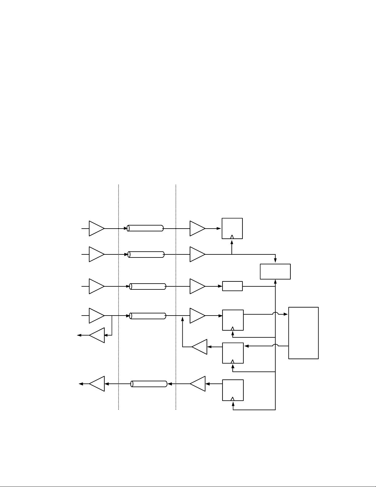
power. Fig. shows the block diagram of LPDDR5 which adopts WCK clocking. WCK
signals are adopted for the write and the read operation in LPDDR5 like GDDR5/6. In
LPDDR4x, as the data rate increases and voltage decrease, the power noise induced jitter
due to long CLK to DQS delay has become the dominant factor to limit the high speed
operation. In order to minimize clock to DQ delay, WCK signals are transmitted to each
byte, meanwhile since WCK signals can be only transmitted during DQ operation to
reduce power consumption, WCK2CK synchronization should be executed for domain
cross between CK and WCK signals whenever read or write commands are issued.
D Q
Memory
Controller
Channel DRAM
(LPDDR5)
CMD/ADDR
(1.6Gbps)
CK_t/CK_c
(800MHz)
WCK_t/WCK_c
(3.2GHz)
DQ
(6.4Gbps)
RDQS
(3.2GHz)
WCK2CK
SYNC
D Q
D Q
D Q
DIV
DRAM
Core
Figure 1: Top-level block diagram of LPDDR5 WCK clocking
剩余24页未读,继续阅读
资源评论

drjiachen
- 粉丝: 172
- 资源: 2138
上传资源 快速赚钱
 我的内容管理
展开
 我的资源
快来上传第一个资源
 我的收益 登录查看自己的收益
 我的积分
登录查看自己的积分
 我的C币
登录后查看C币余额
 我的收藏
我的收藏  我的下载
我的下载  下载帮助
下载帮助

 前往需求广场,查看用户热搜
最新资源
- 疫情下图书馆管理系统-springboot毕业项目,适合计算机毕-设、实训项目、大作业学习.zip
- 在线教育系统-springboot毕业项目,适合计算机毕-设、实训项目、大作业学习.zip
- 已经构建好的CSH初始晶胞,模型经过删除硅链,吸水饱和,基于ClayFF力场,且模型化学组成,密度,钙硅比,Qn分布均与实验值符合,拉伸结果也与文献结果匹配 晶胞文件提供ms文件,可根据具体的模拟需
- 学生网上请假系统设计与实现-springboot毕业项目,适合计算机毕-设、实训项目、大作业学习.rar
- 星之语明星周边产品销售网站的设计与实现-springboot毕业项目,适合计算机毕-设、实训项目、大作业学习.zip
- 中药实验管理系统设计与实现-springboot毕业项目,适合计算机毕-设、实训项目、大作业学习.zip
- 月度员工绩效考核管理系统-springboot毕业项目,适合计算机毕-设、实训项目、大作业学习.rar
- 网页时装购物系统-springboot毕业项目,适合计算机毕-设、实训项目、大作业学习.rar
- 智能学习平台系统-springboot毕业项目,适合计算机毕-设、实训项目、大作业学习.zip
- 校园资料分享平台-springboot毕业项目,适合计算机毕-设、实训项目、大作业学习.rar
- 洗衣店订单管理系统-springboot毕业项目,适合计算机毕-设、实训项目、大作业学习.rar
- 在线教育系统设计与实现-springboot毕业项目,适合计算机毕-设、实训项目、大作业学习.rar
- 学生宿舍管理系统的设计与开发-springboot毕业项目,适合计算机毕-设、实训项目、大作业学习.zip
- 新闻推荐系统-springboot毕业项目,适合计算机毕-设、实训项目、大作业学习.rar
- 小徐影城管理系统-springboot毕业项目,适合计算机毕-设、实训项目、大作业学习.zip
- 学生心理咨询评估系统-springboot毕业项目,适合计算机毕-设、实训项目、大作业学习.rar
资源上传下载、课程学习等过程中有任何疑问或建议,欢迎提出宝贵意见哦~我们会及时处理!
点击此处反馈


安全验证
文档复制为VIP权益,开通VIP直接复制
 信息提交成功