没有合适的资源?快使用搜索试试~ 我知道了~
at91sam9260 nandflash说明文档
5星 · 超过95%的资源 需积分: 35 15 下载量 103 浏览量
2013-12-11
19:45:34
上传
评论 1
收藏 767KB PDF 举报
温馨提示
试读
18页
at91sam9260 关于nand外设的说明文档,9260的data sheet关于nand介绍太少了,这片文章是atmel公司专门为支持nandflash出的说明文档。
资源推荐
资源详情
资源评论
NAND Flash Support in AT91SAM9
Microcontrollers
1. Scope
The purpose of this application note is to introduce the NAND Flash technology and to
describe how to interface NAND Flash memory to Atmel
®
AT91SAM9 ARM
®
Thumb
®
-
based Microcontrollers that do not feature a NAND Flash Controller. The NAND Flash
logic is driven by the Static Memory Controller on the NCS3 address space.
Sample code is provided the associated zip file, Basic NAND Source Code.zip; the
source code is based on the product libV3.
2. NAND Flash Overview
2.1 General Overview
NAND Flash provides a cost effective alternative to hard drives, especially for portable
and handheld systems. The performance, pricing, and memory size options make it
optimal for storage applications
(pictures, audio files, etc.).
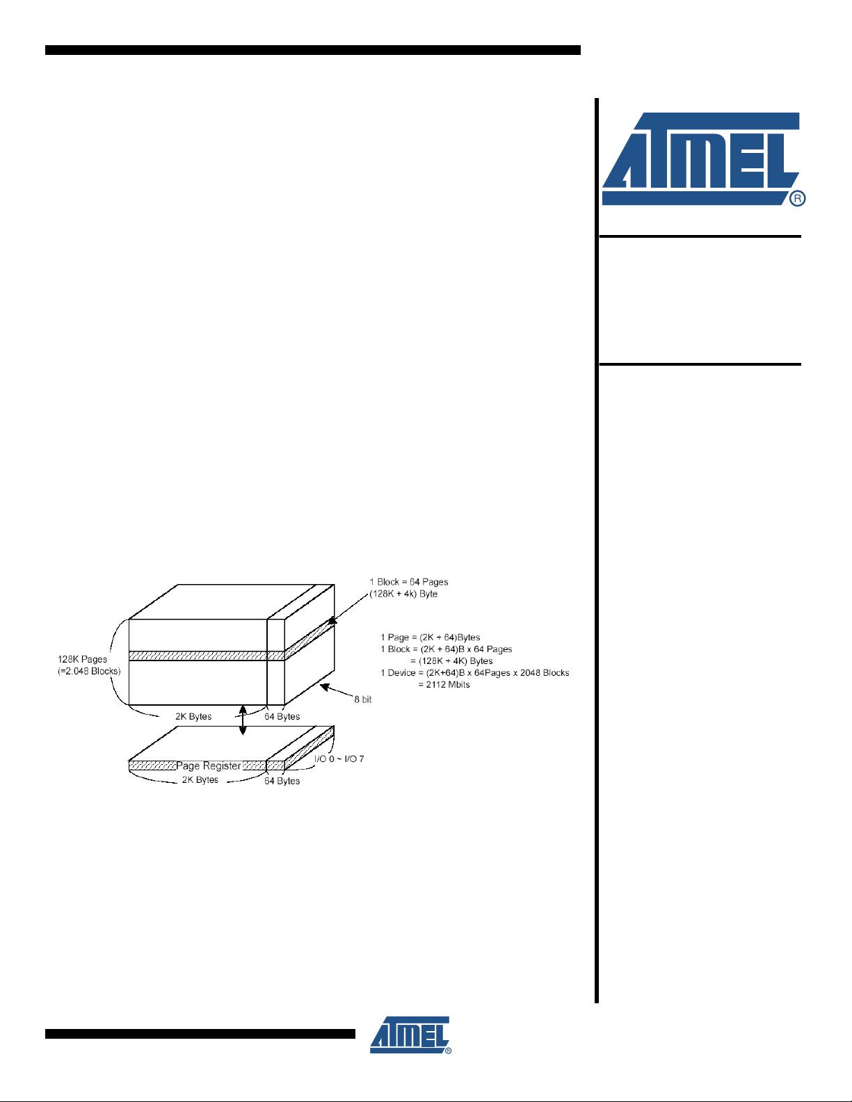
The NAND Flash used to illustrate this interface is the K9F2G08U0M, manufactured
by Samsung
®
Electronics. Figure 2-1 shows the memory organization of this device.
Figure 2-1. K9F2G08U0M Organization
AT91 ARM
Thumb
Microcontrollers
Application
Note
6255B–ATARM–26-Jun-09
2
6255B–ATARM–26-Jun-09
Application Note
2.2 NAND Flash vs. NOR Flash
The most important item for memories is the cost per bit which depends on memory cell area per
bit. The cell area of NAND Flash is smaller than that of NOR Flash, making the NAND Flash
more cost effective than NOR Flash.
The first significant difference between NAND and NOR Flash is the hardware interface.
2.2.1 Hardware Interface
NOR Flash has a fully memory-mapped random access interface similar to a RAM, with dedi-
cated address lines and data lines making it “bootable”.
NAND Flash uses a multiplexed I/O interface and additional control signals. It is controlled by
sending commands and addresses through an 8-bit or 16-bit bus to an internal command and
address register.
NOR Flash random-access interface typically composed of 41 pins:
– CE# - chip enable
– WE# - write enable
– OE# - output enable
– D[15:0] - data bus
– A[20:0] - address bus
– WP# - write protect
NAND Flash I/O device-type interface composed of up to 24 pins:
– CE# - chip enable
– WE# - write enable
– RE# - read enable
– CLE - command latch enable
– ALE - address latch enable
– I/O[7:0] or I/O[15:0] - data bus
– WP# - write protect
– R/B# - ready / busy
– RE - Read enable
2.2.2 Array Architecture
NOR Flash is divided into blocks which typically contain many 16-bit wide words. Random
access to stored data words is achieved by placing the selected word address on the address
bus and then reading that data off the data bus. Erase operations are managed at the block level
and words can be programmed after a block has been erased.
NAND Flash is also divided into blocks which contain many pages instead of words (2K +64
bytes). Read and program operations take place on a per-page basis whereas erase operations
takes place on a block basis.
To read or write from NAND Flash, a command sequence is issued to select a block and a page.
After this selection, the entire page can be read or written.
3
6255B–ATARM–26-Jun-09
Application Note
NAND Flash typically contains blocks that contain errors and cannot be used. A check must be
done by software to list and maintain a table of bad blocks. Data integrity is achieved by using
hardware or software techniques, such as ECC, that check and correct bad data.
2.2.3 Performances
Further differences between NOR and NAND Flash can be found in read/write performances.
Table 2-1 shows random access time for NOR Flash specified at 0.09 µs, whereas NAND ran-
dom access is significantly slower — 25 µs — for the first byte. Once the initial access has been
made, however, the remaining 2,111 bytes are shifted out of NAND at only 30 ns per byte. This
results in a bandwidth of more than 23 Mb/s for 8-bit I/Os or 37 Mb/s for 16-bit I/Os.
The real benefits for NAND Flash can be found in the faster program and erase times, since
NAND provides over five megabytes per second of sustained write performance. The block
erase times are an impressive 2 ms for NAND versus 200 ms for NOR.
2.2.4 Conclusion
Table 2-2 summarizes NAND/NOR advantages and disadvantages.
Clearly, NAND Flash has several significant positive attributes. The one negative attribute is that
it is not well-suited for direct random access.
Table 2-1. Differences in Performance
Characteristics
NAND Flash
K9F2G08U0M
NOR Flash
AT49BV16x4-90
Random access read
25 µs (first byte)
30 ns each for remaining 2111
bytes
0.09 µs
Sustained read speed
(sector basis)
37 Mbytes/s 11 Mbytes/s
Random write speed 300 µs/2,112 bytes 20 µs / bytes
Sustained write speed (sector
basis)
5 Mbytes/s 0.05 Mbytes/s
Erase block size 128 Kbytes 64 Kbytes
Erase cycles 100,000 to 1,000,000 10,000 to 100,000
Erase time per block 2 ms 200 ms
Table 2-2. NAND/NOR Comparison
NAND NOR
Advantages
Fast writes
Fast erases
Lower bit cost
Higher density
Random access
Byte writes possible
Disadvantages
Slow random access
Byte writes difficult
Bad blocks management and ECC
required
Slow writes
Slow erase
Applications
File (disk) applications
Voice, data, video recorder
Any large sequential data
Execute directly from non volatile
memory
4
6255B–ATARM–26-Jun-09
Application Note
NAND is available in large capacities and is the lowest cost Flash memory available today.
NAND is used in virtually all removable cards for cost/density reasons: USB Cards, Memory
Stick, MMC Multimedia Card, SD Secure Digital, CF Compact Flash.
3. Bad Block Management and Error Corrected Code (ECC)
3.1 Definition of “Bad Block”
By default, NAND devices contain invalid blocks which have one or more invalid bits.
Furthermore, since the first memory block (physical block address 00h) in NAND devices is
guaranteed to be free of defects (up to 1,000 PROGRAM/ERASE cycles), the first 8 Kb of Flash
memory can safely be used for system bootstrapping functions.
3.2 Software Considerations
To avoid writing to and reading from bad memory blocks, system software must create a map of
invalid memory blocks. If the application code executes from RAM rather than Flash memory,
system software bad-block mapping is only necessary at boot time and during Flash storage
updates.
All device locations are erased (FFh for X8, FFFFh for X16) except locations where the invalid
block information is written prior to shipping. The invalid block status is defined by the 1st byte
(X8 device) or 1st word (X16 device) in the spare area.
The 1st or 2nd page of every invalid block has non-FFh(X8) or non-FFFFh(X16) data at the col-
umn address of 2048 (X8 device) or 1024 (X16 device). Since the invalid block information is
also erasable in most cases, it is impossible to recover the information once it has been erased.
Therefore, the system must be able to recognize the invalid block(s) based on the original invalid
block information and create the invalid block table via the flow chart in Figure 3-1.
Figure 3-1. Bad Block Recognition Flow Chart
剩余17页未读,继续阅读
资源评论
- vbvc62015-02-03很好用,感谢上传
cxm446749608
- 粉丝: 50
- 资源: 37
上传资源 快速赚钱
- 我的内容管理 展开
- 我的资源 快来上传第一个资源
- 我的收益 登录查看自己的收益
- 我的积分 登录查看自己的积分
- 我的C币 登录后查看C币余额
- 我的收藏
- 我的下载
- 下载帮助
最新资源
- 论文(最终)_20240430235101.pdf
- 基于python编写的Keras深度学习框架开发,利用卷积神经网络CNN,快速识别图片并进行分类
- 最全空间计量实证方法(空间杜宾模型和检验以及结果解释文档).txt
- 5uonly.apk
- 蓝桥杯Python组的历年真题
- 2023-04-06-项目笔记 - 第一百十九阶段 - 4.4.2.117全局变量的作用域-117 -2024.04.30
- 前端开发技术实验报告:内含4四实验&实验报告
- Highlight Plus v20.0.1
- 林周瑜-论文.docx
资源上传下载、课程学习等过程中有任何疑问或建议,欢迎提出宝贵意见哦~我们会及时处理!
点击此处反馈
安全验证
文档复制为VIP权益,开通VIP直接复制
信息提交成功