没有合适的资源?快使用搜索试试~ 我知道了~
lm741运算放大器datasheet.pdf
需积分: 32 11 下载量 168 浏览量
2020-05-01
09:54:43
上传
评论
收藏 722KB PDF 举报
温馨提示
试读
16页
The LM741 series are general-purpose operational amplifiers which feature improved performance over industry standards like the LM709. They are direct,plug-in replacements for the 709C, LM201, MC1439, and 748 in most applications.
资源推荐
资源详情
资源评论
LM741
-
+
V-
V+
+V
supply
R1
V
input
Output
R2
-V
supply
Product
Folder
Sample &
Buy
Technical
Documents
Tools &
Software
Support &
Community
LM741
SNOSC25D –MAY 1998–REVISED OCTOBER 2015
LM741 Operational Amplifier
1 Features 3 Description
The LM741 series are general-purpose operational
1
• Overload Protection on the Input and Output
amplifiers which feature improved performance over
• No Latch-Up When the Common-Mode Range is
industry standards like the LM709. They are direct,
Exceeded
plug-in replacements for the 709C, LM201, MC1439,
and 748 in most applications.
2 Applications
The amplifiers offer many features which make their
• Comparators
application nearly foolproof: overload protection on
the input and output, no latch-up when the common-
• Multivibrators
mode range is exceeded, as well as freedom from
• DC Amplifiers
oscillations.
• Summing Amplifiers
The LM741C is identical to the LM741 and LM741A
• Integrator or Differentiators
except that the LM741C has their performance
• Active Filters
ensured over a 0°C to +70°C temperature range,
instead of −55°C to +125°C.
Device Information
(1)
PART NUMBER PACKAGE BODY SIZE (NOM)
TO-99 (8) 9.08 mm × 9.08 mm
LM741 CDIP (8) 10.16 mm × 6.502 mm
PDIP (8) 9.81 mm × 6.35 mm
(1) For all available packages, see the orderable addendum at
the end of the data sheet.
Typical Application
1
An IMPORTANT NOTICE at the end of this data sheet addresses availability, warranty, changes, use in safety-critical applications,
intellectual property matters and other important disclaimers. PRODUCTION DATA.
LM741
SNOSC25D –MAY 1998–REVISED OCTOBER 2015
www.ti.com
Table of Contents
7.3 Feature Description................................................... 7
1 Features.................................................................. 1
7.4 Device Functional Modes.......................................... 8
2 Applications ........................................................... 1
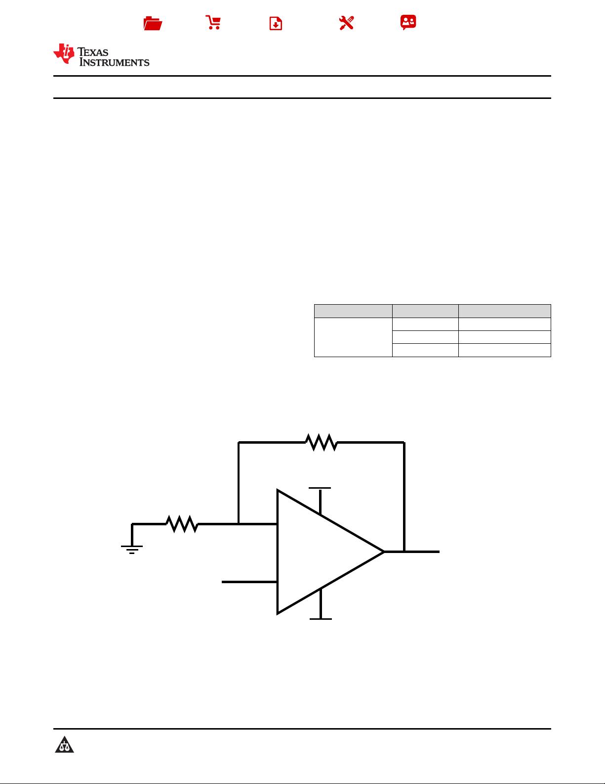
8 Application and Implementation .......................... 9
3 Description ............................................................. 1
8.1 Application Information.............................................. 9
4 Revision History..................................................... 2
8.2 Typical Application ................................................... 9
5 Pin Configuration and Functions......................... 3
9 Power Supply Recommendations...................... 10
6 Specifications......................................................... 4
10 Layout................................................................... 11
6.1 Absolute Maximum Ratings ...................................... 4
10.1 Layout Guidelines ................................................. 11
6.2 ESD Ratings.............................................................. 4
10.2 Layout Example .................................................... 11
6.3 Recommended Operating Conditions....................... 4
11 Device and Documentation Support ................. 12
6.4 Thermal Information.................................................. 4
11.1 Community Resources.......................................... 12
6.5 Electrical Characteristics, LM741.............................. 5
11.2 Trademarks........................................................... 12
6.6 Electrical Characteristics, LM741A ........................... 5
11.3 Electrostatic Discharge Caution............................ 12
6.7 Electrical Characteristics, LM741C ........................... 6
11.4 Glossary................................................................ 12
7 Detailed Description .............................................. 7
12 Mechanical, Packaging, and Orderable
7.1 Overview ................................................................... 7
Information ........................................................... 12
7.2 Functional Block Diagram ......................................... 7
4 Revision History
NOTE: Page numbers for previous revisions may differ from page numbers in the current version.
Changes from Revision C (October 2004) to Revision D Page
• Added Applications section, Pin Configuration and Functions section, ESD Ratings table, Feature Description
section, Device Functional Modes, Application and Implementation section, Power Supply Recommendations
section, Layout section, Device and Documentation Support section, and Mechanical, Packaging, and Orderable
Information section ................................................................................................................................................................ 1
• Removed NAD 10-Pin CLGA pinout ..................................................................................................................................... 3
• Removed obselete M (S0-8) package from the data sheet ................................................................................................... 4
• Added recommended operating supply voltage spec ............................................................................................................ 4
• Added recommended operating temperature spec ................................................................................................................ 4
Changes from Revision C (March 2013) to Revision D Page
• Added Applications section, Pin Configuration and Functions section, ESD Ratings table, Feature Description
section, Device Functional Modes, Application and Implementation section, Power Supply Recommendations
section, Layout section, Device and Documentation Support section, and Mechanical, Packaging, and Orderable
Information section ................................................................................................................................................................ 1
• Removed NAD 10-Pin CLGA pinout ..................................................................................................................................... 3
• Removed obselete M (S0-8) package from the data sheet ................................................................................................... 4
• Added recommended operating supply voltage spec ............................................................................................................ 4
• Added recommended operating temperature spec ................................................................................................................ 4
2 Submit Documentation Feedback Copyright © 1998–2015, Texas Instruments Incorporated
Product Folder Links: LM741
LM741
www.ti.com
SNOSC25D –MAY 1998–REVISED OCTOBER 2015
5 Pin Configuration and Functions
LMC Package
NAB Package
8-Pin TO-99
8-Pin CDIP or PDIP
Top View
Top View
LM741H is available per JM38510/10101
Pin Functions
PIN
I/O DESCRIPTION
NAME NO.
INVERTING
2 I Inverting signal input
INPUT
NC 8 N/A No Connect, should be left floating
NONINVERTING
3 I Noninverting signal input
INPUT
OFFSET NULL
1, 5 I Offset null pin used to eliminate the offset voltage and balance the input voltages.
OFFSET NULL
OUTPUT 6 O Amplified signal output
V+ 7 I Positive supply voltage
V– 4 I Negative supply voltage
Copyright © 1998–2015, Texas Instruments Incorporated Submit Documentation Feedback 3
Product Folder Links: LM741
LM741
SNOSC25D –MAY 1998–REVISED OCTOBER 2015
www.ti.com
6 Specifications
6.1 Absolute Maximum Ratings
over operating free-air temperature range (unless otherwise noted)
(1)(2)(3)
MIN MAX UNIT
LM741, LM741A ±22
Supply voltage V
LM741C ±18
Power dissipation
(4)
500 mW
Differential input voltage ±30 V
Input voltage
(5)
±15 V
Output short circuit duration Continuous
LM741, LM741A –50 125
Operating temperature °C
LM741C 0 70
LM741, LM741A 150
Junction temperature °C
LM741C 100
PDIP package (10 seconds) 260
°C
Soldering information
CDIP or TO-99 package (10 seconds) 300
°C
Storage temperature, T
stg
–65 150 °C
(1) Stresses beyond those listed under Absolute Maximum Ratings may cause permanent damage to the device. These are stress ratings
only, which do not imply functional operation of the device at these or any other conditions beyond those indicated under Recommended
Operating Conditions. Exposure to absolute-maximum-rated conditions for extended periods may affect device reliability.
(2) For military specifications see RETS741X for LM741 and RETS741AX for LM741A.
(3) If Military/Aerospace specified devices are required, please contact the TI Sales Office/Distributors for availability and specifications.
(4) For operation at elevated temperatures, these devices must be derated based on thermal resistance, and T
j
max. (listed under “Absolute
Maximum Ratings”). T
j
= T
A
+ (θ
jA
P
D
).
(5) For supply voltages less than ±15 V, the absolute maximum input voltage is equal to the supply voltage.
6.2 ESD Ratings
VALUE UNIT
V
(ESD)
Electrostatic discharge Human body model (HBM), per ANSI/ESDA/JEDEC JS-001
(1)
±400 V
(1) Level listed above is the passing level per ANSI, ESDA, and JEDEC JS-001. JEDEC document JEP155 states that 500-V HBM allows
safe manufacturing with a standard ESD control process.
6.3 Recommended Operating Conditions
over operating free-air temperature range (unless otherwise noted)
MIN NOM MAX UNIT
LM741, LM741A ±10 ±15 ±22
Supply voltage (VDD-GND) V
LM741C ±10 ±15 ±18
LM741, LM741A –55 125
Temperature °C
LM741C 0 70
6.4 Thermal Information
LM741
THERMAL METRIC
(1)
LMC (TO-99) NAB (CDIP) P (PDIP) UNIT
8 PINS 8 PINS 8 PINS
R
θJA
Junction-to-ambient thermal resistance 170 100 100 °C/W
R
θJC(top)
Junction-to-case (top) thermal resistance 25 — — °C/W
(1) For more information about traditional and new thermal metrics, see the Semiconductor and IC Package Thermal Metrics application
report, SPRA953.
4 Submit Documentation Feedback Copyright © 1998–2015, Texas Instruments Incorporated
Product Folder Links: LM741
剩余15页未读,继续阅读
资源评论
aren207
- 粉丝: 3
- 资源: 15
上传资源 快速赚钱
- 我的内容管理 展开
- 我的资源 快来上传第一个资源
- 我的收益 登录查看自己的收益
- 我的积分 登录查看自己的积分
- 我的C币 登录后查看C币余额
- 我的收藏
- 我的下载
- 下载帮助
安全验证
文档复制为VIP权益,开通VIP直接复制
信息提交成功