没有合适的资源?快使用搜索试试~ 我知道了~
资源详情
资源评论
资源推荐
LP2997
June 29, 2012
DDR-II Termination Regulator
General Description
The LP2997 linear regulator is designed to meet the JEDEC
SSTL-18 specifications for termination of DDR-II memory.
The device contains a high-speed operational amplifier to
provide excellent response to load transients. The output
stage prevents shoot through while delivering 500mA contin-
uous current and transient peaks up to 900mA in the appli-
cation as required for DDR-II SDRAM termination. The
LP2997 also incorporates a V
SENSE
pin to provide superior
load regulation and a V
REF
output as a reference for the
chipset and DIMMs.
An additional feature found on the LP2997 is an active low
shutdown (SD
) pin that provides Suspend To RAM (STR)
functionality. When SD is pulled low the V
TT
output will tri-
state providing a high impedance output, but, V
REF
will remain
active. A power savings advantage can be obtained in this
mode through lower quiescent current.
Features
■
Source and sink current
■
Low output voltage offset
■
No external resistors required
■
Linear topology
■
Suspend to Ram (STR) functionality
■
Low external component count
■
Thermal Shutdown
■
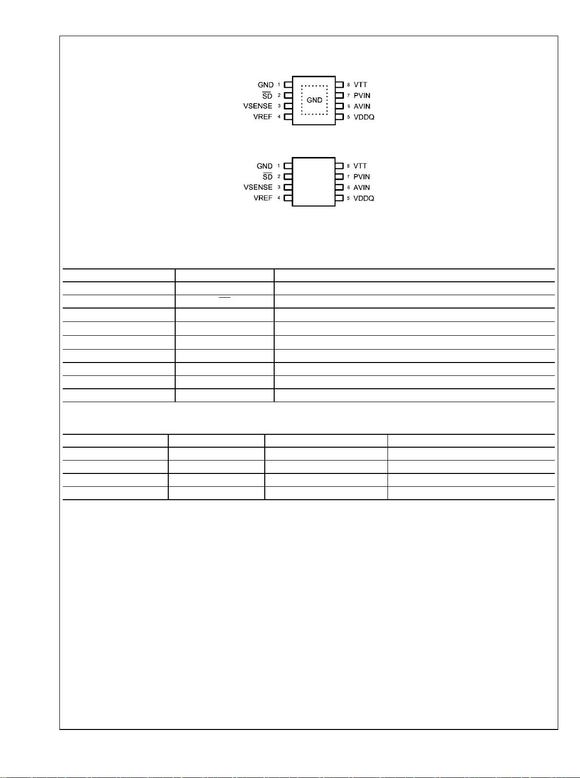
Available in SO-8, PSOP-8 packages
Applications
■
DDR-II Termination Voltage
■
SSTL-18 Termination
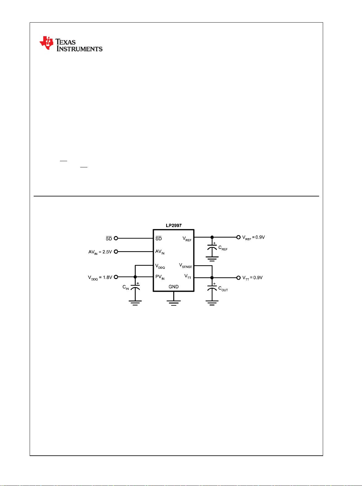
Typical Application Circuit
20109418
© 2012 Texas Instruments Incorporated 201094 SNVS295E www.ti.com
LP2997 DDR-II Termination Regulator
Connection Diagrams
20109403
PSOP-8 Layout
20109404
SO-8 Layout
Pin Descriptions
SO-8 Pin or PSOP-8 Pin Name Function
1 GND Ground
2 SD Shutdown
3 VSENSE Feedback pin for regulating V
TT
.
4 VREF Buffered internal reference voltage of V
DDQ
/2
5 VDDQ Input for internal reference equal to V
DDQ
/2
6 AVIN Analog input pin
7 PVIN Power input pin
8 VTT Output voltage for connection to termination resistors
EP Exposed pad thermal connection Connect to Ground
Ordering Information
Order Number Package Type NSC Package Drawing Supplied As
LP2997M SO-8 M08A 95 Units per Rail
LP2997MX SO-8 M08A 2500 Units Tape and Reel
LP2997MR PSOP-8 MRA08A 95 Units Tape and Reel
LP2997MRX PSOP-8 MRA08A 2500 Units Tape and Reel
www.ti.com 2
LP2997
Absolute Maximum Ratings (Note 1)
If Military/Aerospace specified devices are required,
please contact the Texas Instruments Sales Office/
Distributors for availability and specifications.
AVIN to GND −0.3V to +6V
PVIN to GND -0.3V to AVIN
VDDQ (Note 2) −0.3V to +6V
Storage Temp. Range −65°C to +150°C
Junction Temperature 150°C
Lead Temperature (Soldering, 10 sec) 260°C
SO-8 Thermal Resistance (θ
JA
)
151°C/W
PSOP-8 Thermal Resistance (θ
JA
)
43°C/W
Minimum ESD Rating (Note 3) 1kV
Operating Range
Junction Temp. Range (Note 4) 0°C to +125°C
AVIN to GND 2.2V to 5.5V
Electrical Characteristics Specifications with standard typeface are for T
J
= 25°C and limits in boldface type
apply over the full Operating Temperature Range (T
J
= 0°C to +125°C) (Note 5). Unless otherwise specified,
AVIN = 2.5V, PVIN = 1.8V, VDDQ = 1.8V.
Symbol Parameter Conditions Min Typ Max Units
V
REF
V
REF
Voltage PVIN = VDDQ = 1.7V
PVIN = VDDQ = 1.8V
PVIN = VDDQ = 1.9V
0.837
0.887
0.936
0.860
0.910
0.959
0.887
0.937
0.986
V
Z
VREF
V
REF
Output Impedance
I
REF
= -30 to +30 μA
2.5
kΩ
V
TT
V
TT
Output Voltage I
OUT
= 0A
PVIN = VDDQ = 1.7V
PVIN = VDDQ = 1.8V
PVIN = VDDQ = 1.9V
0.822
0.874
0.923
0.856
0.908
0.957
0.887
0.939
0.988
V
I
OUT
= ±0.5A (Note 8)
PVIN = VDDQ = 1.7V
PVIN = VDDQ = 1.8V
PVIN = VDDQ = 1.9V
0.828
0.878
0.928
0.856
0.908
0.957
0.890
0.940
0.990
Vos
TT
/V
TT
V
TT
Output Voltage Offset
(V
REF
-V
TT
)
I
OUT
= 0A
I
OUT
= -0.5A
I
OUT
= +0.5A
-25
-25
-25
0
0
0
25
25
25
mV
I
Q
Quiescent Current (Note 6) I
OUT
= 0A (Note 6) 320 500
µA
Z
VDDQ
VDDQ Input Impedance 100
kΩ
I
SD
Quiescent Current in
Shutdown (Note 6)
SD = 0V 115 150 µA
I
Q_SD
Shutdown Leakage Current SD = 0V 2 5 µA
V
IH
Minimum Shutdown High
Level
1.9 V
V
IL
Maximum Shutdown Low
Level
0.8 V
I
SENSE
V
SENSE
Input Current 13 nA
T
SD
Thermal Shutdown (Note 7) 165 Celsius
T
SD
_HYS Thermal Shutdown
Hysteresis
10 Celsius
3 www.ti.com
LP2997
Note 1: Absolute maximum ratings indicate limits beyond which damage to the device may occur. Operating range indicates conditions for which the device is
intended to be functional, but does not guarantee specific performance limits. For guaranteed specifications and test conditions see Electrical Characteristics.
The guaranteed specifications apply only for the test conditions listed. Some performance characteristics may degrade when the device is not operated under
the listed test conditions.
Note 2: VDDQ voltage must be less than 2 x (AVIN - 1) or 6V, whichever is smaller.
Note 3: The human body model is a 100pF capacitor discharged through a 1.5kΩ resistor into each pin.
Note 4: At elevated temperatures, devices must be derated based on thermal resistance. The device in the SO-8 package must be derated at θ
JA
= 151.2° C/W
junction to ambient with no heat sink.
Note 5: Limits are 100% production tested at 25°C. Limits over the operating temperature range are guaranteed through correlation using Statistical Quality
Control (SQC) methods. The limits are used to calculate National's Average Outgoing Quality Level (AOQL).
Note 6: Quiescent current defined as the current flow into AVIN.
Note 7: The maximum allowable power dissipation is a function of the maximum junction temperature, T
J(MAX)
, the junction to ambient thermal resistance, θ
JA
,
and the ambient temperature, T
A
. Exceeding the maximum allowable power dissipation will cause excessive die temperature and the regulator will go into thermal
shutdown.
Note 8: V
TT
load regulation is tested by using a 10 ms current pulse and measuring V
TT
.
www.ti.com 4
LP2997
Typical Performance Characteristics
Iq vs AV
IN
in SD
20109420
Iq vs AV
IN
20109421
V
IH
and V
IL
20109422
V
REF
vs V
DDQ
20109424
V
TT
vs V
DDQ
20109426
Iq vs AV
IN
in SD Temperature
20109427
5 www.ti.com
LP2997
剩余21页未读,继续阅读
aqjinhu
- 粉丝: 0
- 资源: 2
上传资源 快速赚钱
- 我的内容管理 展开
- 我的资源 快来上传第一个资源
- 我的收益 登录查看自己的收益
- 我的积分 登录查看自己的积分
- 我的C币 登录后查看C币余额
- 我的收藏
- 我的下载
- 下载帮助
最新资源
- docker一键安装包
- Screenshot_20240430_144340_com.ss.android.ugc.live.jpg
- 回到山沟沟.mp3
- 基于matlab实现自适应波束形成RLS及LMS算法仿真源程序1.rar
- 基于matlab实现自己编写的基于卡尔曼滤波的利用加速度传感器的计步器,测试数据是传感器放在腰部和手臂 .rar
- 基于matlab实现阵列信号处理,波束形成.rar
- 111111111111111111
- 基于matlab实现计步器编程;对当前的计步器装置的数值算法模拟 .rar
- Mdb学习查看PW;access;mdb;pw;password;patch
- 基于matlab实现关于语音信号声源定位DOA估计所用的一些传统算法.rar
资源上传下载、课程学习等过程中有任何疑问或建议,欢迎提出宝贵意见哦~我们会及时处理!
点击此处反馈
安全验证
文档复制为VIP权益,开通VIP直接复制
信息提交成功
评论0