没有合适的资源?快使用搜索试试~ 我知道了~
资源推荐
资源详情
资源评论
This quick reference guide presents the following step-by-step flows for
quickly closing timing, based on the recommendations in the UltraFast
Design Methodology Guide for Xilinx FPGAs and SoCs (UG949):
Initial Design Checks: Review utilization, logic levels, and timing
constraints before implementing the design.
Timing Baselining: Review and address timing violations after each
implementation step to help close timing after routing.
Timing Violation Resolution: Identify the root cause of setup or hold
violations, and resolve the timing violations.
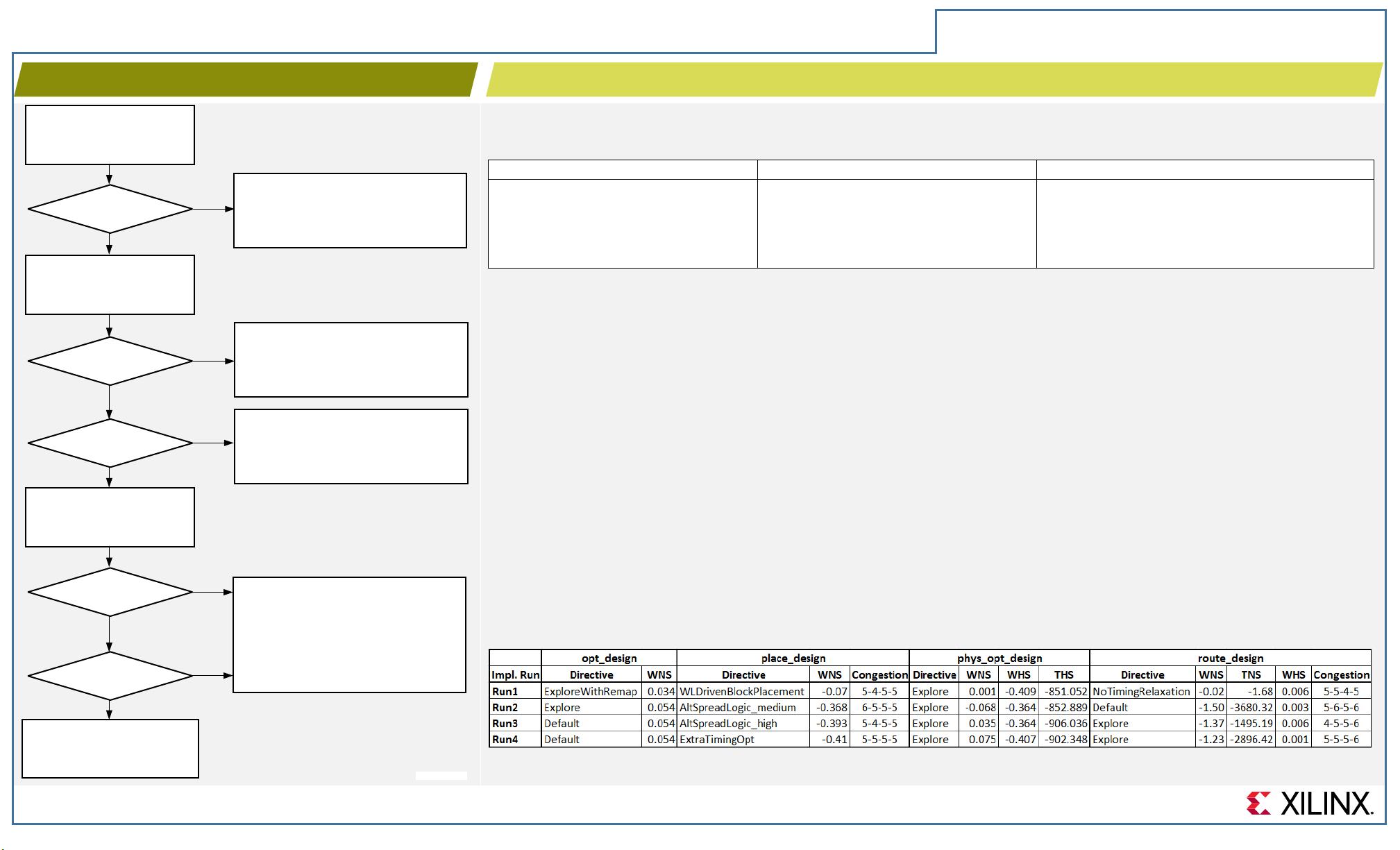
Failfast and QoR Assessment Reports
You can use the failfast and quality of results (QoR) assessment reports
interchangeably to quickly review your design. Both reports compare
key design and constraints metrics against guideline limits. Metrics that
do not comply with guidelines are marked as REVIEW. The reports
include the following sections:
Design characteristics
Methodology checks
Conservative logic-level assessments based on a target Fmax
In the Vivado® tools, you can run these reports as follows:
xilinx::designutils::report_failfast
report_qor_assessment
See Failfast Report Overview (page 10) and the Vivado Design Suite
User Guide: Design Analysis and Closure Techniques (UG906).
QoR Suggestions Report
In the Vivado tools, report_qor_suggestions is called during the
implementation phase. This report analyzes the design, offers
suggestions, and automatically applies the suggestions in some cases.
Reports in the Vitis Environment
In the Vitis™ environment, report_failfast is called during the
compilation flow when using v++ –R 1 or v++ –R 2. To generate QoR
assessment and suggestions in the Vivado tools, use:
v++ --interactive
TIP: To automatically address most timing closure challenges during
implementation, you can use an Intelligent Design Run (IDR), which
is a special type of implementation run that leverages
report_qor_suggestions, ML-based strategy predictions, and
incremental compile. See UG949: Using Intelligent Design Runs.
Although implementing a design on a Xilinx® device is a fairly automated
task, achieving higher performance and resolving compilation issues due
to timing or routing violations can be a complex and time-consuming
activity. It can be difficult to identify the reason for a failure based on
simple log messages or post-implementation timing reports generated
by the tools. Therefore, it is essential to adopt a step-by-step design
development and compilation methodology, including the review of
intermediate results to ensure the design can proceed to the next
implementation step.
The first step is to make sure all initial design checks are addressed.
Review these checks at the following levels:
Each kernel made of custom RTL or generated by Vivado HLS
Note: Check that target clock frequency constraints are realistic.
Each major hierarchy corresponding to a subsystem, such as a
Vivado IP integrator block diagram with several kernels, IP blocks,
and connectivity logic
Complete design with all major functions and hierarchies, I/O
interfaces, complete clocking circuitry, and physical and timing
constraints
If the design uses floorplanning constraints, such as super logic region
(SLR) assignments or logic assigned to Pblocks, review the estimated
resource utilization for each physical constraint, and make sure that the
utilization guidelines are met. See the default guidelines in the failfast
report. To generate reports, use the following commands:
report_utilization –pblocks <pblockName>
report_failfast –pblock <pblockName>
report_failfast [–slr SLRn | -by_slr]
UG1292 (v2021.2) November 19, 2021
1
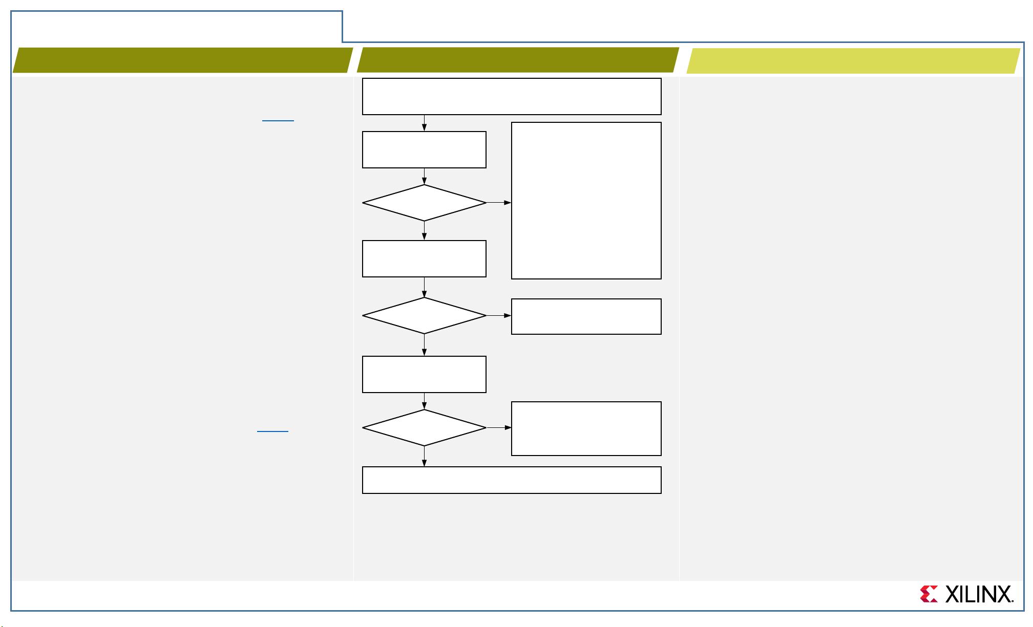
Open the synthesized design checkpoint (DCP) or the post-opt_design DCP
(if available)
Run report_failfast
Review Check Timing section in
report_timing_summary
Run report_methodology
Proceed to design implementation (logic optimization, placement, routing)
Fix methodology checks that impact
timing closure (Fmax)
Create missing clock constraints to
eliminate unconstrained internal
endpoints and avoid timing loops
Review the detailed reports to identify
the design characteristics or
constraints to improve:
● Estimated device and SLR Pblock
resource utilization
● Constraints preventing optimizations
● Control signals and average fanout
● Clock tree and clock domain
crossing constraints
● High logic levels given the target
frequency
Clean report?
Clean report?
Clean report?
Yes
Yes
Yes
No
No
No
X21574-091818
INTRODUCTION
INITIAL DESIGN CHECKS - DETAILS
INITIAL DESIGN CHECKS FLOW
INITIAL DESIGN CHECKS DETAILS
UltraFast Design Methodology Timing Closure
Quick Reference Guide (UG1292)
The objective of timing baselining is to ensure that the design meets timing by analyzing and resolving timing challenges after each
implementation step. Fixing the design and constraints issues earlier in the compilation flow ensures a broader impact and higher performance.
Review and address timing violations before moving onto the next step by creating intermediate reports as follows:
Reports in Vivado Project Mode
Reports in Vivado Non-Project Mode
Reports in the Vitis Software Platform
Use the UltraFast™ design methodology
or timing closure report strategies
Add the following report commands after
each implementation step:
report_timing_summary
report_methodology
report_failfast
Use the
v++ -R 1
or
v++ -R 2
option to generate
failfast reports, intermediate timing reports, and
DCPs in the following directory:
<runDir>/_x/link/vivado/prj/prj.runs/impl_1
Pre-Placement (WNS < 0 ns)
Before place_design, the timing report reflects the design performance assuming the best possible logic placement for each logic path. Setup
violations must be addressed by adopting the Initial Checks recommendations.
Pre-Routing (WNS < 0 ns)
Before route_design, the timing report reflects the design performance assuming the best possible routing delays for each individual net with
some fanout penalty and without considering hold fixing impact (net routing detours) or congestion. Setup violations are often due to sub-
optimal placement caused by (1) high device or SLR utilization, (2) placement congestion due to complex logic connectivity, (3) many paths with
many logic levels, and (4) high clock skew between unbalanced clocks or high clock uncertainty. Run phys_opt_design in Explore or
AggressiveExplore mode to try improving the post-place_design QoR. If unsuccessful, focus on improving the placement QoR first.
Pre-Routing (WHS < -0.5 ns)
When the performance goal is not met after routing and worst negative slack (WNS) is positive before routing, try to reduce large estimated
worst hold slack (WHS) violations. Fewer and smaller pre-route hold violations help route_design focus on Fmax rather than fixing hold time
violations.
Post-Routing (WNS < 0 ns or WHS < 0 ns)
After route_design, first verify that the design is fully routed by reviewing the log files or running report_route_status on the post-route
design checkpoint (DCP). Routing violations and large setup (WNS) or hold (WHS) violations are the result of high congestion. Use the Analyzing
Setup Violations (page 3), Resolving Hold Violations (page 4), and Congestion Reduction Techniques (page 6) to identify and implement the
resolution steps. Try running phys_opt_design after route_design to address small setup violations > -0.200 ns.
When iterating the design, constraints, and compilation strategies, keep track of the QoR after each step, including the congestion information.
Use the QoR table to compare run characteristics and determine what to focus on first when addressing the remaining timing violations.
TIP: Use report_qor_suggestions after place_design and after route_design to automatically identify design, constraints, and tool option
changes that can help improve the QoR for new compilations.
UG1292 (v2021.2) November 19, 2021
2
Generate bitstream and run
design on the Xilinx device
See Post-Routing (WNS < 0 ns or
WHS < 0 ns) (this page)
WNS > 0 ns?
See Pre-Routing (WHS < -0.5 ns) (this
page)
See Pre-Routing (WNS < 0 ns) (this page)
See Pre-Placement (WNS < 0 ns) (this
page)
Open the synthesized design
checkpoint, run
opt_design
,
and run
report_timing_summary
Run
place_design
,
phys_opt_design
(optional),
and
report_timing_summary
Run
route_design
,
phys_opt_design
(optional),
and
report_timing_summary
WNS > 0 ns?
WHS > -0.5 ns?
WNS > 0 ns?
WHS > 0 ns?
No
Yes
No
No
No
No
Yes
Yes
Yes
Yes
X21575-091818
TIMING BASELINING FLOW
TIMING BASELINING EXAMPLE
UltraFast Design Methodology Timing Closure
Quick Reference Guide (UG1292)
Design performance is determined by the following:
Clock skew and clock uncertainty: How efficiently the clocks are
implemented
Logic delay: Amount of logic traversed during a clock cycle
Net or route delay: How efficiently Vivado implementation places
and routes the design
Use the information in the timing path or design analysis reports to:
Identify which of these factors contributes most to timing violations
Determine how to iteratively improve the QoR
TIP: If needed, open the DCP after each step to generate additional
reports.
In Vivado project mode, find setup timing path characteristics as follows:
1. In the Design Runs window, select the implementation run to analyze.
2. In the Implementation Run Properties window, select the Reports tab.
3. Open the timing summary report or design analysis report for the selected implementation step:
Timing summary report: <runName>_<flowStep>_report_timing_summary (.rpt for text or .rpx for the Vivado IDE)
Design analysis report: <runName>_<flowStep>_report_design_analysis
In Vivado non-project mode or in the Vitis software platform, do either of the following:
Open the reports in the implementation run directory.
Open the implementation DCP in the Vivado IDE, and open the RPX version of the report.
Note: Using the Vivado IDE allows you to cross-probe between the reports, schematics, and Device window.
For each timing path, the logic delay, route delay, clock skew, and clock uncertainty characteristics are located in the header of the path:
The same timing path characteristics are located in the Setup Path Characteristics of the design analysis report along with additional
information, such as Logic Levels and Routes:
TIP: In text mode, all columns of the Setup Path Characteristics column appear, making the table very wide. In the Vivado IDE, the same table
shows a reduced number of columns to help with visualization. Right-click the table header to enable or disable columns as needed. For
example, the DONT_TOUCH or MARK_DEBUG columns are not visible by default. Enable these columns to view important information skipped
logic optimization analysis, which is difficult to identify otherwise.
UG1292 (v2021.2) November 19, 2021
3
Logic delay > 50%
of datapath delay?
Open the timing report, identify the worst violating paths for each clock group, and
apply the following step-by-step analysis to each of the paths
Net delay > 50%
of datapath delay?
Clock skew < -0.5 ns?
Clock uncertainty > 0.100 ns?
See Reducing Logic
Delay (page 5)
See Reducing Net Delay
(pages 6 and 7)
See Improving Clock
Skew (page 8)
See Improving Clock
Uncertainty (page 9)
Yes
Yes
Yes
Yes
X21576-091818
ANALYZING SETUP VIOLATIONS FLOW
FINDING SETUP TIMING PATH CHARACTERISTICS IN THE REPORTS
UltraFast Design Methodology Timing Closure
Quick Reference Guide (UG1292)
剩余10页未读,继续阅读
资源评论
MyStefanieLove
- 粉丝: 0
- 资源: 1
上传资源 快速赚钱
- 我的内容管理 展开
- 我的资源 快来上传第一个资源
- 我的收益 登录查看自己的收益
- 我的积分 登录查看自己的积分
- 我的C币 登录后查看C币余额
- 我的收藏
- 我的下载
- 下载帮助
最新资源
- libjpeg 编译所需的 Win32.mak vs编译libjpeg
- 自动驾驶-状态估计和定位-粒子滤波实现和源码.pdf
- 数据可视化-智慧物流服务中心大屏页面.zip
- yolov5,SSD 可能使用到的一些代码
- bbbbbbbbbbbbbbbbbb
- 安卓逆向学习笔记之Frida Stalker 还原OLLVM AES.docx
- 安卓逆向学习笔记之unicorn来trace还原OLLVM Base64.docx
- 基于jquery的自定义表格组件实现
- Nessus最新20240426离线安装插件all-2.0.tar.gz
- 最新版本私钥助记词碰撞器大富豪使用python进行制作通过接口的方式进行验证支持多币种多链多网络一分钟万次验证高出货率
资源上传下载、课程学习等过程中有任何疑问或建议,欢迎提出宝贵意见哦~我们会及时处理!
点击此处反馈
安全验证
文档复制为VIP权益,开通VIP直接复制
信息提交成功