HY64UD16162B Series
2
Revision 1.0 / December. 2002
This document is a general product description and is subject to change without notice. Hynix Semiconductor Inc. does not
assume any responsibility for use of circuits described. No patent licenses are implied.
1
1
M x 16 bit Low
M x 16 bit Low
Low Power 1T/1C
Low Power 1T/1C
SRAM
SRAM
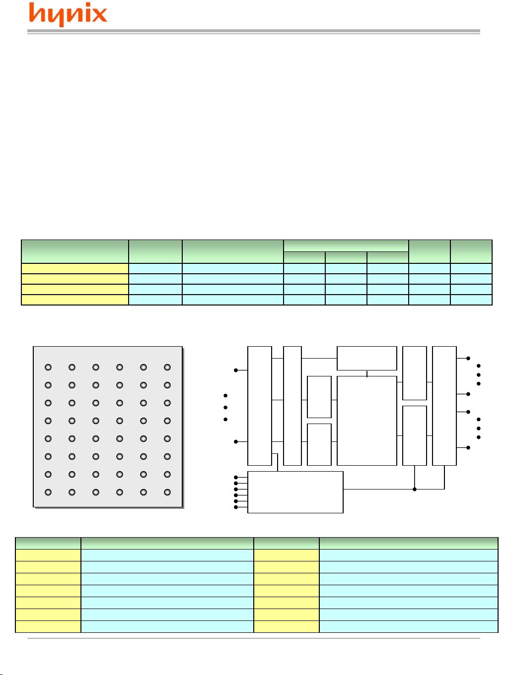
DESCRIPTION
The HY64UD16162B is a 16Mbit 1T/1C SRAM
featured by high-speed operation and super low
power consumption. The HY64UD16162B adopts
one transistor memory cell and is organized as
1,048,576 words by 16bits. The HY64UD16162B
operates in the extended range of temperature and
supports a wide operating voltage range. The
HY64UD16162B also supports the deep power
down mode for a super low standby current. The
HY64UD16162B delivers the high-density low
power SRAM capability to the high-speed low power
system.
• CMOS Process Technology
• 1M x 16 bit Organization
• TTL compatible and Tri-state outputs
• Deep Power Down : Memory cell data hold invalid
• Standard pin configuration : 48-FBGA(6mmX8mm)
• Data mask function by /LB, /UB
• Separated I/O Power Supply : Vddq
PRODUCT FAMILY
FEATURES
Note 1. tCS - /UB,/LB=High : Chip Deselect.
PIN DESCRIPTION
Pin Name Pin Function Pin Name Pin Function
/CS1 Chip Select
IO1~IO8 Lower Data Inputs/Outputs
/WE Write Enable
A0~A19 Address Inputs
/OE Output Enable
Vdd Power Supply for Internal Circuit
/LB Lower Byte(I/O1~I/O8)
Vss Ground
/UB Upper Byte(I/O9~I/O16)
CS2 Deep Power Down
DNU Do Not Use
IO9~IO16 Upper Data Inputs/Outputs
Vddq Power Supply for I/O
NC No Connection
PIN CONNECTION (Top View)
/LB /OE A0 A1 A2 CS2
IO9 /UB A3 A4 /CS1 IO1
IO10 IO11 A5 A6 IO2 IO3
Vss IO12 A17 A7 IO4 Vdd
Vddq IO13 DNU A16 IO5 Vss
IO15 IO14 A14 A15 IO6 IO7
IO16 A19 A12 A13 /WE IO8
A18 A8 A9 A10 A11 NC
BLOCK DIAGRAM
ADD INPUT
BUFFER
PRE DECODER
COLUMN
DECODER
BLOCK
DECODER
ROW
DECODER
SENSE AMP WRITE DRIVER
DATA I/O
BUFFER
MEMORY ARRAY
1,024K x 16
CONTROL
LOGIC
A0
A19
IO1
IO8
IO9
IO16
/CS1
CS2
/OE
/LB
/UB
/WE
Product No.
Voltage [V]
Vdd/Vddq
Speed
tRC[ns]
Temp.
[°C]
(ISB1,Max) (IDPD,Max) (ICC2,Max)
Power Dissipation
Mode
HY64UD16162B-DF70E 3.0/3.0 70 -25~8585µA 2µA 25mA1CS with /UB,/LB:tCS
1
HY64UD16162B-DF60E 3.0/3.0 TBD -25~85TBD 2µA 25mA1CS with /UB,/LB:tCS
1
HY64UD16162B-DF60I 3.0/3.0 TBD -40~85TBD 2µA 25mA1CS with /UB,/LB:tCS
1
HY64UD16162B-DF70I 3.0/3.0 70 -40~8585µA 2µA 25mA1CS with /UB,/LB:tCS
1


评论0