


AEC - Q100-006 - REV-D
July 18, 2003
Component Technical Committee
Automotive Electronics Council
ATTACHMENT 6
AEC - Q100-006 REV-D
ELECTRO-THERMALLY INDUCED PARASITIC GATE LEAKAGE TEST
(GL)

AEC - Q100-006 - REV-D
July 18, 2003
Component Technical Committee
Automotive Electronics Council
Acknowledgment
Any document involving a complex technology brings together experience and skills from many sources. The
Automotive Electronics Counsel would especially like to recognize the following significant contributors to the
development of this document:
Mark A. Kelly Delphi Delco Electronics Systems

AEC - Q100-006 - REV-D
July 18, 2003
Component Technical Committee
Automotive Electronics Council
Change Notification
The following summary details the changes incorporated into AEC-Q100-006 Rev-D:
• Sections 3.5, 3.5.1, and 3.5.2: Deleted section title 3.5, Detailed Procedure. Changed
section 3.5.1 to section 3.5 and section 3.5.2 to section 3.6.
AEC - Q100-006 - REV-D
July 18, 2003
Component Technical Committee
Automotive Electronics Council
DaimlerChrysler Date Delphi Delco Electronics Systems Date Visteon Corporation Date
Majdi Mortazavi Detlef Griessman Robert V. Knoell
Copyright © 2003 by DaimlerChrysler, Delphi Delco Electronics Systems, and Visteon Corporation. This document may be freely
reprinted with this copyright notice. This document cannot be changed without approval by the AEC Component Technical Committee.
Page 1 of 12
METHOD - 006
ELECTRO-THERMALLY INDUCED PARASITIC
GATE LEAKAGE (GL) TEST
Text enhancements and differences made since the last revision of this
document are shown as underlined areas.
1. SCOPE
1.1 Description
The purpose of this specification is to establish a reliable and repeatable procedure for determining
surface mount integrated circuit susceptibility to Electro-Thermally Induced Parasitic Gate Leakage
(GL). This specification may also be used as an evaluation tool for determining the susceptibility of
circuit designs, molding compounds, fabrication processes, and post mold cure processes to GL.
1.2 Reference Documents
Not applicable.
1.3 Terms and Definitions
The terms used in this specification are defined as follows:
1.3.1 Device Failure
A condition in which a device does not meet all the requirements of the acceptance criteria, as
specified in section 5, following the GL test.
1.3.2 DUT
An electronic device being evaluated for its sensitivity to GL.
1.3.3 Electro-Thermally Induced Parasitic Gate Leakage (GL)
A trapped-charge phenomenon affecting plastic encapsulated integrated circuits in varying degrees
depending upon circuit design, fabrication technology, molding compound, and post mold cure profile.
The phenomena occurs at high temperature when an electric field (E-field) is present. GL results in
yield losses during high temperature processes, especially those with heated air flow (e.g., high
temperature handling and IR reflow solder operations). The phenomena can be detected as an
increase in Icc, input leakage, pin parametrics degradation, or functional failure. GL does not cause
permanent damage and can be reversed by a 4 hour unbiased bake at a temperature of 125 °C (or 2
hours at 150 °C).
AEC - Q100-006 - REV-D
July 18, 2003
Component Technical Committee
Automotive Electronics Council
Page 2 of 12
1.3.4 Electro-Thermally Induced Parasitic Gate Leakage (GL) Sensitivity
A GL level resulting in device failure. Sensitivity will vary depending upon the design, layout,
process, and materials used.
2. EQUIPMENT
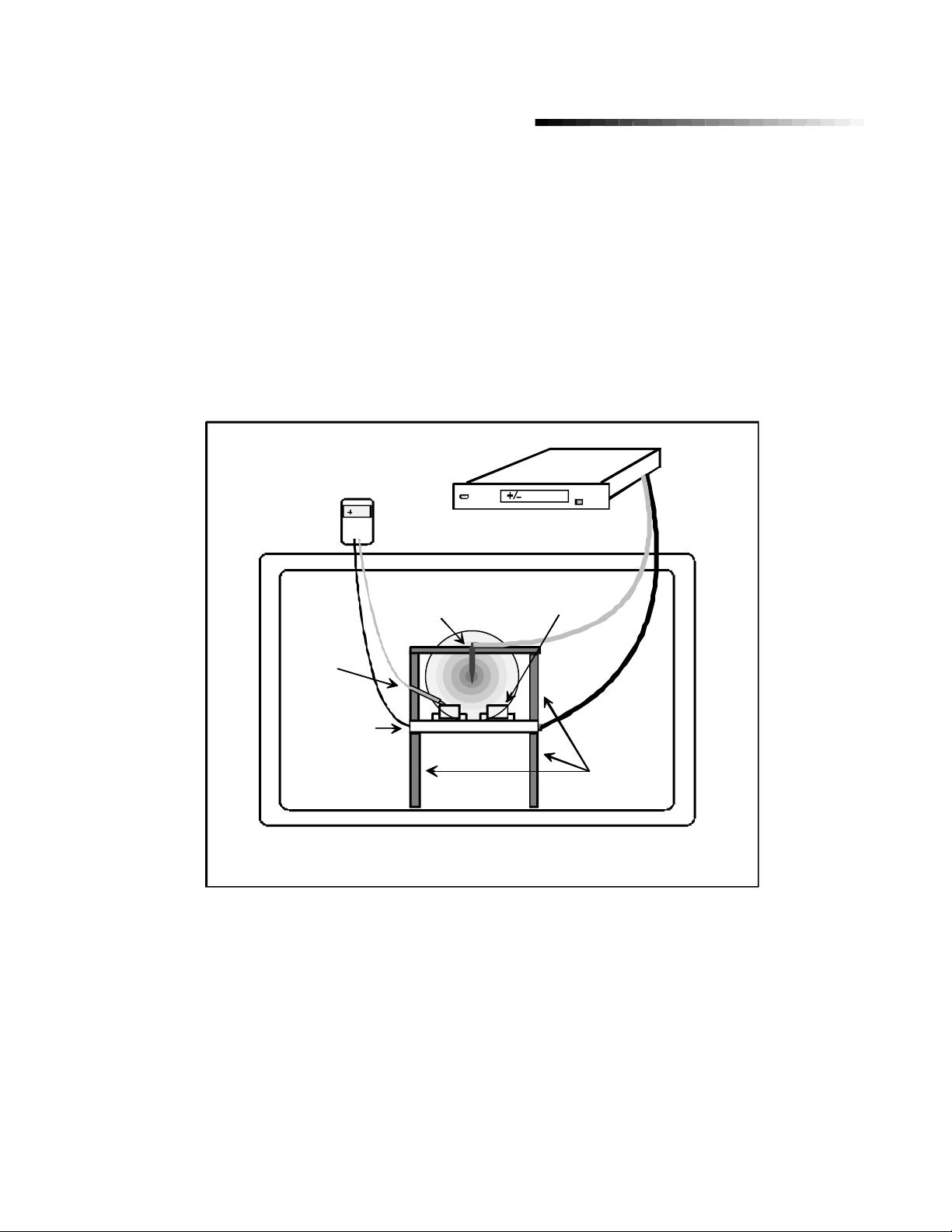
2.1 Test Apparatus
The apparatus required for this test consists of a GL test fixture, high voltage power supply, and
thermal chamber. Figure 1 shows an equivalent test setup.
0 to 20 KV dual polarity
Thermal Chamber
Digital
voltmeter
High
voltage
probe
Pointed
tungsten probe
Conductive
base plate
Insulating
supports
Device
under test
400
11,000 V
DC power supply
Figure 1: GL Test Fixture and Set-up
2.1.1 GL Test Fixture
A test fixture as illustrated in Figure 1 and Appendix A. Other equivalent test fixture configurations
may be used, but the actual fixture must meet the following requirements:
1. The tungsten probe must be at a height of 2.5 ± 0.5 inches above the conductive base plate
surface and allow for vertical movement to facilitate voltage adjustment.
2. To ensure consistent test results, all test devices must be able to be repeatably placed
with leads in contact with the conductive base plate surface by using milled recesses or
equivalent markings and shall be equidistant from the high voltage tungsten probe.


