Complete, Quad, 12-/14-/16-Bit, Serial Input,
Unipolar/Bipolar Voltage Output DACs
AD5724/AD5734/AD5754
Rev. 0
Information furnished by Analog Devices is believed to be accurate and reliable. However, no
responsibility is assumed by Analog Devices for its use, nor for any infringements of patents or other
rights of third parties that may result from its use. Specifications subject to change without notice. No
license is granted by implication or otherwise under any patent or patent rights of Analog Devices.
Trademarks and registered trademarks are the property of their respective owners.
One Technology Way, P.O. Box 9106, Norwood, MA 02062-9106, U.S.A.
Tel: 781.329.4700 www.analog.com
Fax: 781.461.3113 ©2008 Analog Devices, Inc. All rights reserved.
FEATURES
Complete, quad, 12-/14-/16-bit digital-to-analog converter
(DAC)
Operates from single/dual supplies
Software programmable output range
+5 V, +10 V, +10.8 V, ±5 V, ±10 V, ±10.8 V
INL error: ±16 LSB maximum, DNL error: ±1 LSB maximum
Total unadjusted error (TUE): 0.1% FSR maximum
Settling time: 10 μs typical
Integrated reference buffers
Output control during power-up/brownout
Simultaneous updating via
LDAC
Asynchronous
CLR
to zero scale or midscale
DSP-/microcontroller-compatible serial interface
24-lead TSSOP
Operating temperature range: −40°C to +85°C
iCMOS process technology
1
APPLICATIONS
Industrial automation
Closed-loop servo control, process control
Automotive test and measurement
Programmable logic controllers
GENERAL DESCRIPTION
The AD5724/AD5734/AD5754 are quad, 12-/14-/16-bit, serial
input, voltage output digital-to-analog converters. They operate
from single-supply voltages from +4.5 V up to +16.5 V or dual-
supply voltages from ±4.5 V up to ±16.5 V. Nominal full-scale
output range is software-selectable from +5 V, +10 V, +10.8 V,
±5 V, ±10 V, or ±10.8 V. Integrated output amplifiers, reference
buffers, and proprietary power-up/power-down control circuitry
are also provided.
The parts offer guaranteed monotonicity, integral nonlinearity
(INL) of ±16 LSB maximum, low noise, and 10 μs maximum
settling time.
The AD5724/AD5734/AD5754 use a serial interface that operates
at clock rates up to 30 MHz and are compatible with DSP and
microcontroller interface standards. Double buffering allows
the simultaneous updating of all DACs. The input coding is
user-selectable twos complement or offset binary for a bipolar
output (depending on the state of Pin BIN/
2sComp
), and straight
binary for a unipolar output. The asynchronous clear function
clears all DAC registers to a user-selectable zero-scale or midscale
output. The parts are available in a 24-lead TSSOP and offer
guaranteed specifications over the −40°C to +85°C industrial
temperature range.
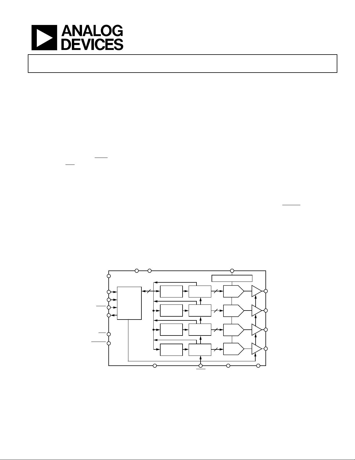
FUNCTIONAL BLOCK DIAGRAM
0
6468-001
DAC C
DAC D
DAC B
INPUT
REGISTER A
INPUT
REGISTER B
INPUT
REGISTER C
nn
DAC A
LDAC
REFIN
V
OUT
D
V
OUT
C
V
OUT
B
V
OUT
A
REFERENCE BUFFERS
SDIN
SCLK
SYNC
SDO
CLR
DV
CC
GND
n
n
n
BIN/2sCOMP
DAC_GND (2) SIG_GND (2)
AD5724/AD5734/AD5754
INPUT SHIFT
REGISTER
AND
CONTROL
LOGIC
A
V
DD
AV
SS
INPUT
REGISTER D
DAC
REGISTER A
DAC
REGISTER B
DAC
REGISTER C
DAC
REGISTER D
AD5724: n = 12-BIT
AD5734: n = 14-BIT
AD5754: n = 16-BIT
Figure 1.
1
For analog systems designers within industrial/instrumentation equipment OEMs who need high performance ICs at higher-voltage levels, iCMOS® is a technology
platform that enables the development of analog ICs capable of 30 V and operating at ±15 V supplies while allowing dramatic reductions in power consumption and
package size, as well as increased ac and dc performance.


