没有合适的资源?快使用搜索试试~ 我知道了~
EP5358LUI/EP5358HUI 600mA Synchronous Buck Regulator with Integ
需积分: 1 0 下载量 150 浏览量
2024-01-26
10:00:06
上传
评论
收藏 234KB PDF 举报
温馨提示
试读
16页
EP5358LUI/EP5358HUI 600mA Synchronous Buck Regulator with Integ
资源推荐
资源详情
资源评论
03541 09/23/2010 Rev: D
EP5358LUI/EP5358HUI
600mA Synchronous Buck Regulator
with Integrated Inductor
RoHS Compliant; Halogen Free
www.enpirion.com
Description
The EP5358xUI (x = L or H) is rated for up to
600mA of continuous output current. The
EP5358xUI integrates MOSFET switches,
control, compensation, and the magnetics in an
advanced 2.5mm x 2.25mm micro-QFN
Package.
Integrated magnetics enables a tiny solution
footprint, low output ripple, low part-count, and
high reliability, while maintaining high efficiency.
The complete solution can be implemented in as
little as 12mm
2
.
The EP5358xUI uses a 3-pin VID to easily select
the output voltage setting. Output voltage
settings are available in 2 optimized ranges
providing coverage for typical V
OUT
settings.
The VID pins can be changed on the fly for fast
dynamic voltage scaling. EP5358LUI further has
the option to use an external voltage divider.
The EP5358xUI is a perfect solution for noise
sensitive and space constrained applications that
require high efficiency.
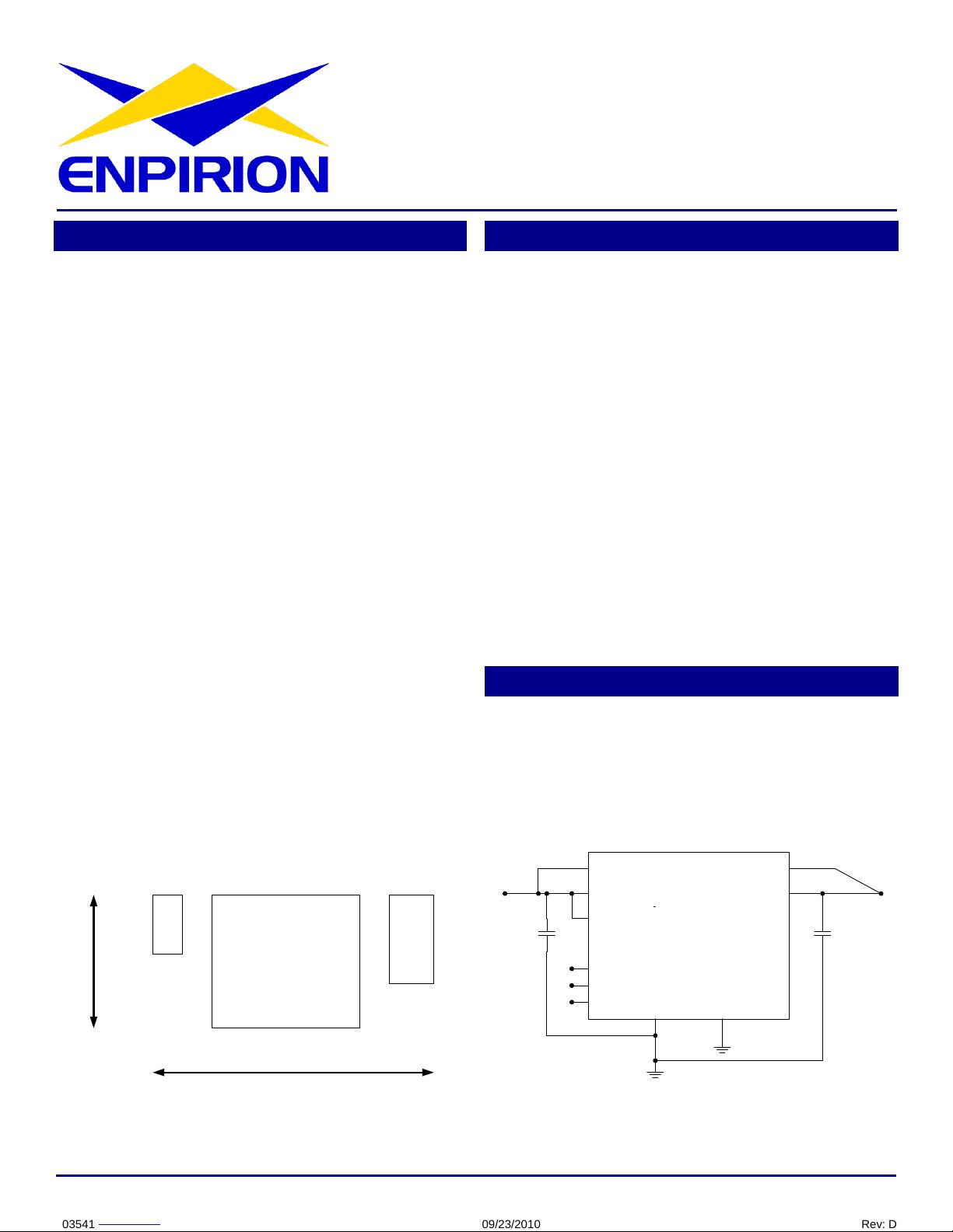
EP5358xUI
2.2uF
10uF
4.75mm
2.25mm
Figure 1: Total Solution Footprint.
Features
• Integrated Inductor Technology
• 2.5mm x 2.25mm x 1.1mm uQFN package
• Total Solution Footprint 12mm
2
• Low V
OUT
ripple for RF compatibility
• High efficiency, up to 93%
• Up to 600mA continuous output current
• Less than 1µA standby current
• 5 MHz switching frequency
• 3 pin VID for glitch free voltage scaling
• V
OUT
Range 0.6V to V
IN
– 0.25V
• Short circuit and over current protection
• UVLO and thermal protection
• IC level reliability in a PowerSOC solution
Application
• Wireless and RF applications
• Wireless broad band data cards
• Smart phone and portable media players
• Advanced Low Power Processors, DSP, IO,
Memory, Video, Multimedia Engines
V
OUT
2.2uF
PGND
EP5358HUI
ENABLE
PV
IN
V
S0
V
S1
V
S2
V
SENSE
V
OUT
10uF
AGND
AV
IN
V
IN
Figure 2: Typical Application Schematic
Downloaded from Elcodis.com electronic components distributor
03541 09/23/2010 Rev: D
EP5358LUI/EP5358HUI
Enpirion 2010 all rights reserved, E&OE 2 www.enpirion.com
Ordering Information
Part Number Comment Package
EP5358LUI LOW VID Range 16-pin QFN T&R
EP5358HUI HIGH VID Range 16-pin QFN T&R
EP5358LUI-E EP5358LUI Evaluation Board
EP5358HUI-E EP5358HUI Evaluation Board
Pin Assignments (Top View)
PVIN
AVIN
ENABLE
VS0
VS1
VS2
NC(SW)
PGND
PGND
VFB
VSENSE
AGND
VOUT
VOUT
NC(SW)
NC(SW)
EP5358LUI
3
1
4
2
6
5
16 15
7 8
12
11
13
10
9
14
Figure 3: EP5358LUI Pin Out Diagram (Top View)
PVIN
AVIN
ENABLE
VS0
VS1
VS2
NC(SW)
PGND
PGND
NC
VSENSE
AGND
VOUT
VOUT
NC(SW)
NC(SW)
EP5358HUI
3
1
4
2
6
5
16 15
7 8
12
11
13
10
9
14
Figure 4: EP5358HUI Pin Out Diagram (Top View)
Pin Description
PIN
NAME
FUNCTION
1, 15,
16
NC(SW)
NO CONNECT – These pins are internally connected to the common switching node of the
internal MOSFETs. NC (SW) pins are not to be electrically connected to any external signal,
ground, or voltage. However, they must be soldered to the PCB. Failure to follow this
guideline may result in part malfunction or damage to the device.
2,3 PGND
Power ground. Connect these pins together and to the ground electrode of the Input and
output filter capacitors.
4 VFB/NC
EP5358LUI: Feed back pin for external divider option.
EP5358HUI: No Connect
5 VSENSE Sense pin for preset output voltages. Refer to application section for proper configuration.
6 AGND
Analog ground. This is the quiet ground for the internal control circuitry, and the ground
return for external feedback voltage divider
7, 8 VOUT Regulated Output Voltage. Refer to application section for proper layout and decoupling.
9, 10,
11
VS2, VS1,
VS0
Output voltage select. VS2 = pin 9, VS1 = pin 10, VS0 = pin 11.
EP5358LUI: Selects one of seven preset output voltages or an external resistor divider.
EP5358HUI: Selects one of eight preset output voltages.
(Refer to section on output voltage select for more details.)
12 ENABLE Output Enable. Enable = logic high; Disable = logic low
13 AVIN Input power supply for the controller circuitry.
14 PVIN Input Voltage for the MOSFET switches.
Downloaded from Elcodis.com electronic components distributor
03541 09/23/2010 Rev: D
EP5358LUI/EP5358HUI
Enpirion 2010 all rights reserved, E&OE 3 www.enpirion.com
Absolute Maximum Ratings
CAUTION: Absolute Maximum ratings are stress ratings only. Functional operation beyond the
recommended operating conditions is not implied. Stress beyond the absolute maximum ratings may
cause permanent damage to the device. Exposure to absolute maximum rated conditions for
extended periods may affect device reliability.
PARAMETER
SYMBOL
MIN
MAX
UNITS
Input Supply Voltage V
IN
-0.3 6.0 V
Voltages on: ENABLE, V
SENSE
, V
SO
– V
S2
-0.3 V
IN
+ 0.3 V
Voltages on: V
FB
(EP5358LUI)
-0.3 2.7 V
Maximum Operating Junction Temperature T
J-ABS
150 °C
Storage Temperature Range T
STG
-65 150 °C
Reflow Temp, 10 Sec, MSL3 JEDEC J-STD-020C 260 °C
ESD Rating (based on Human Body Mode) 2000 V
Recommended Operating Conditions
PARAMETER
SYMBOL
MIN
MAX
UNITS
Input Voltage Range V
IN
2.4 5.5 V
Operating Ambient Temperature T
A
-40 +85 °C
Operating Junction Temperature T
J
-40 +125 °C
Thermal Characteristics
PARAMETER
SYMBOL
TYP
UNITS
Thermal Resistance: Junction to Ambient –0 LFM (Note 1)
θ
JA
85 °C/W
Thermal Overload Trip Point T
J-TP
+155 °C
Thermal Overload Trip Point Hysteresis 25 °C
Note 1: Based on a four layer copper board and proper thermal design per JEDEC EIJ/JESD51 standards
Downloaded from Elcodis.com electronic components distributor
03541 09/23/2010 Rev: D
EP5358LUI/EP5358HUI
Enpirion 2010 all rights reserved, E&OE 4 www.enpirion.com
Electrical Characteristics
NOTE: T
A
= -40°C to +85°C unless otherwise noted. Typical v alues are at T
A
= 25°C, VIN = 3.6V.
C
IN
= 4.7µF MLCC, C
OUT
= 10µF
PARAMETER
SYMBOL
TEST CONDITIONS
MIN
TYP
MAX
UNITS
Operating Input Voltage
Range
V
IN
2.4 5.5 V
Under Voltage Lock-out –
V
IN
Rising
V
UVLO_R
2.0 V
Under Voltage Lock-out –
V
IN
Falling
V
UVLO_F
1.9 V
Drop Out Resistance R
DO
Input to Output Resistance in 100%
duty cycle operation.
350 500 mΩ
Output Voltage Range
V
OUT
EP5358LUI (V
DO
= I
LOAD
X R
DO
)
EP5358HUI
0.6
1.8
V
IN
-V
DO
3.3
V
Dynamic Voltage Slew
Rate (VID Change)
V
SLEW
EP5358LUI
EP5358HUI
4
8
V/mS
VID Preset V
OUT
Initial
Accuracy
∆V
OUT
T
A
= 25°C, V
IN
= 3.6V;
I
LOAD
= 100mA ;
0.8V ≤ V
OUT
≤ 3.3V
-2 +2 %
Line Regulation
∆V
OUT_LINE
2.4V ≤ V
IN
≤ 5.5V 0.03 %/V
Load Regulation
∆V
OUT_LOAD
0A ≤ I
LOAD
≤ 600mA 0.48 %/A
Temperature Variation
∆V
OUT_TEMPL
-40°C ≤ T
A
≤ +85°C
24
ppm/°C
Output Current I
OUT
600 mA
Shut-down Current I
SD
Enable = Low 0.75 µA
OCP Threshold I
LIM
2.4V ≤ V
IN
≤ 5.5V
0.6V ≤ V
OUT
≤ 3.3V
1.25 1.4 A
Feedback Pin Voltage
Initial Accuracy
V
FB
T
A
= 25°C, V
IN
= 3.6V;
I
LOAD
= 100mA ;
0.8V ≤ V
OUT
≤ 3.3V
.588 0.6 0.612 V
Feedback Pin Input
Current
I
FB
Note 1 <100 nA
VS0-VS2, Pin Logic Low V
VSLO
0.0 0.3 V
VS0-VS2, Pin Logic High V
VSHI
1.4
V
IN
V
VS0-VS2, Pin Input
Current
I
VSX
Note 1 <100 nA
Enable Pin Logic Low V
ENLO
0.3 V
Enable Pin Logic High V
ENHI
1.4 V
Enable Pin Current I
ENABLE
Note 1 <100 nA
Operating Frequency F
OSC
5 MHz
Soft Start Operation
Soft Start Slew Rate
∆V
SS
EP5358LUI (VID MODE)
EP5358HUI (VID MODE)
2.6
5.2
4
8
5.4
10.8
V/mS
V
OUT
Rise Time T
RISE
EP53A8LUI VFB MODE 146 225 304 uSec
Note 1: Parameter guaranteed by design
Downloaded from Elcodis.com electronic components distributor
剩余15页未读,继续阅读
资源评论
南山言射频
- 粉丝: 221
- 资源: 6
上传资源 快速赚钱
- 我的内容管理 展开
- 我的资源 快来上传第一个资源
- 我的收益 登录查看自己的收益
- 我的积分 登录查看自己的积分
- 我的C币 登录后查看C币余额
- 我的收藏
- 我的下载
- 下载帮助
安全验证
文档复制为VIP权益,开通VIP直接复制
信息提交成功